TA2015FNG Ver la hoja de datos (PDF) - Toshiba
Número de pieza
componentes Descripción
Fabricante
TA2015FNG Datasheet PDF : 8 Pages
| |||
TA2015FNG
Application Note
1. Operation mode of constant current source
Operation mode is decided by switch condition shown in
table.1. Output of constant current source 1 can be used
as a reset circuit by changing start up timing of PW SW,
MODE SW.
2. Ripple filter output
It is necessary to connect an external pull−down resistor
with PW SW (pin(6)) and MODE SW (pin(5)) in case that
ripple filter circuit doesn’t operate normally due to
external noise etc.
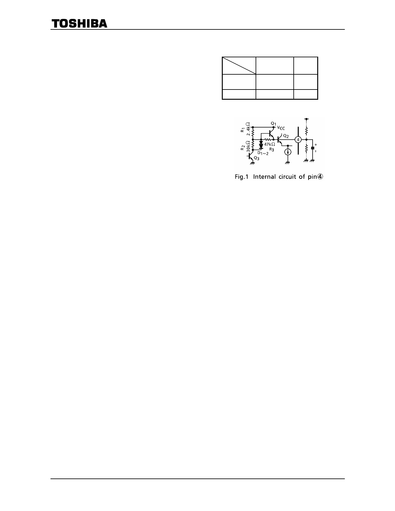
3. Adjustment of ripple filter output voltage
Internal circuit of pin(4) is shown in Fig.1. Ripple filter
output voltage is decided by internal resistor R1, R2 and
Q3, and limited by D1~2 and Q3 to VRF = 1.5V (typ.)
Ripple filter output voltage can be controlled by method
below.
Mode
SW
H
L
PW SW
H
IO2
IO1
RF OUT
IO2
L
—
—
Table.1 Operation mode
(1) Method to rise the ripple filter output voltage
External resistor should be connected between VCC and RF
IN terminal (pin(4)). In this case, output current capacity of
ripple filter circuit is down. Because at ripple filter output
stage, collector−emitter voltage of PNP transistor will small,
and drive capacity of transistor is down.
(2) Method to drop the ripple filter output voltage
External resistor should be connected between GND and RF IN terminal (pin(4)).
Current flows through external resistor and internal resistor R1, R3 (2.4kΩ, 47kΩ).
In case that output voltage dropped too much, ripple rejection ratio and other characteristics will be worse,
because constant current source of differential amplifier is saturated especially at low voltage.
3
2004-10-12
Share Link: 