TA2015FNG Ver la hoja de datos (PDF) - Toshiba
Número de pieza
componentes Descripción
Fabricante
TA2015FNG Datasheet PDF : 8 Pages
| |||
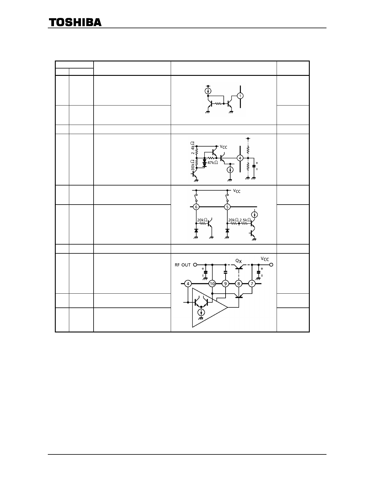
Terminal Explanation
Terminal Voltage: Typical Terminal Voltage with Test Circuit
(VCC = 1.2V, Ta = 25°C, non load)
Terminal
No. Name
1
IO1
2
IO2
3
GND
Function
Output of constant current
source 1
Operating condition
PW SW : H
MODE SW : L
Output of constant current
source 2
Synchronized to PW SW
—
Internal Circuit
—
Ripple filter terminal
Ripple filter output voltage
4
RF in
can be controlled by external
resistor.
(See application note)
Mode switch
5 Mode SW
VCC
: IO2, RF OUT on
GND / OPEN : IO1, IO2 on
Power switch
6 PW SW
VCC
: Power on
GND / OPEN : Power off
7
VCC
—
—
Base biasing terminal for ripple
filter transistor.
Output current capacity is
8
Base
1.2mA with only built−in PNP
transistor.
This capacity can be increased
with an external transistor QX.
9
Comp
Phase compensation terminal for
a ripple filter circuit
10 RF out Ripple filter output
TA2015FNG
Terminal
Voltage (V)
—
—
0
1.14
—
—
1.2
0.5
0.5
1.14
2
2004-10-12
Share Link: 