CY74FCT162501ATPAC Ver la hoja de datos (PDF) - Cypress Semiconductor
Número de pieza
componentes Descripción
Fabricante
CY74FCT162501ATPAC Datasheet PDF : 7 Pages
| |||
1CY 74FCT1 62H5 01
T
fax id: 7047
CY74FCT16501T
CY74FCT162501T
CY74FCT162H501T
Features
18-Bit Registered Transceiver
Functional Description
• Low power, pin-compatible replacement for ABT
functions
• FCT-E speed at 3.8 ns
• Power-off disable outputs permits live insertion
• Edge-rate control circuitry for significantly improved
noise characteristics
• Typical output skew < 250 ps
• ESD > 2000V
• TSSOP (19.6 mil pitch) and SSOP (25-mil pitch)
packages
• Extended commercial range of −40°C to +85°C
• VCC = 5V ± 10%
CY74FCT16501T Features:
• 64 mA sink current, 32 mA source current
• Typical VOLP (ground bounce) <1.0V at VCC = 5V,
TA = 25°C
CY74FCT162501T Features:
• Balanced output drivers: 24 mA
• Reduced system switching noise
• Typical VOLP (ground bounce) <0.6V at VCC = 5V,
TA= 25°C
CY74FCT162H501T Features:
• Bus hold retains last active state
• Eliminates the need for external pull-up or pull-down
resistors
These 18-bit universal bus transceivers can be operated in
transparent, latched or clock modes by combining D-type
latches and D-type flip-flops. Data flow in each direction is
controlled by output enable (OEAB and OEBA), latch enable
(LEAB and LEBA), and clock inputs (CLKAB and CLKBA). For
A-to-B data flow, the device operates in transparent mode
when LEAB is HIGH. When LEAB is LOW, the A data is latched
if CLKAB is held at a HIGH or LOW logic level. If LEAB is LOW,
the A bus data is stored in the latch/flip-flop on the
LOW-to-HIGH transition of CLKAB. OEAB performs the output
enable function on the B port. Data flow from B-to-A is similar
to that of A-to-B and is controlled by OEBA, LEBA, and CLKBA.
The output buffers are designed with a power-off disable fea-
ture to allow live insertion of boards.
The CY74FCT16501T is ideally suited for driving
high-capacitance loads and low-impedance backplanes.
THE CY74FCT162501T has 24-mA balanced output drivers
with current limiting resistors in the outputs. This reduces the
need for external terminating resistors and provides for minimal
undershoot and reduced ground bounce. The
CY74FCT162501T is ideal for driving transmission lines.
The CY74FCT162H501T is a 24-mA balanced output part, that
has “bus hold” on the data inputs. The device retains the input’s
last state whenever the input goes to high impedance. This
eliminates the need for pull-up/down resistors and prevents
floating inputs.
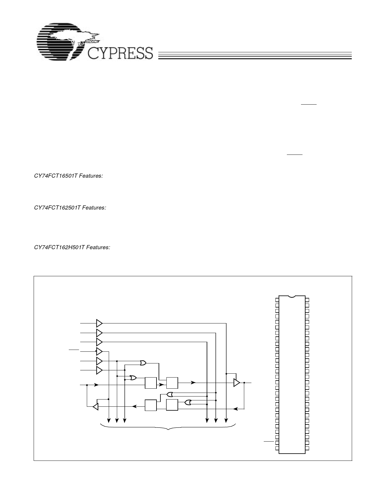
Functional Block Diagram
OEAB
CLKBA
LEBA
OEBA
CLKAB
LEAB
A1
C
C
D
D
C
C
D
D
TO 17 OTHER CHANNELS
FCT16501-1
Pin Configuration
SSOP/TSSOP
Top View
OEAB 1
LEAB 2
A1 3
GND 4
A2 5
A3 6
VCC 7
A4 8
A5 9
A 6 10
GND 11
A 7 12
A 8 13
A 9 14
A10 15
B1
A11 16
A12 17
GND 18
A13 19
A14 20
A15 21
VCC 22
A16 23
A17 24
GND 25
A18 26
OEBA 27
LEBA 28
56 GND
55 CLKAB
54 B1
53 GND
52 B2
51 B3
50 VCC
49 B4
48 B5
47 B6
46 GND
45 B7
44 B8
43 B9
42 B10
41 B11
40 B12
39 GND
38 B13
37 B14
36 B15
35 VCC
34 B16
33 B17
32 GND
31 B18
30 CLKBA
29 GND
FCT16501-2
Cypress Semiconductor Corporation • 3901 North First Street • San Jose • CA 95134 • 408-943-2600
August 19994 – Revised March 18, 1997
Share Link: 