SD103A Ver la hoja de datos (PDF) - Vishay Semiconductors
Número de pieza
componentes Descripción
Fabricante
SD103A Datasheet PDF : 4 Pages
| |||
www.vishay.com
SD103A, SD103B, SD103C
Vishay Semiconductors
Small Signal Schottky Diodes
DESIGN SUPPORT TOOLS click logo to get started
Models
Available
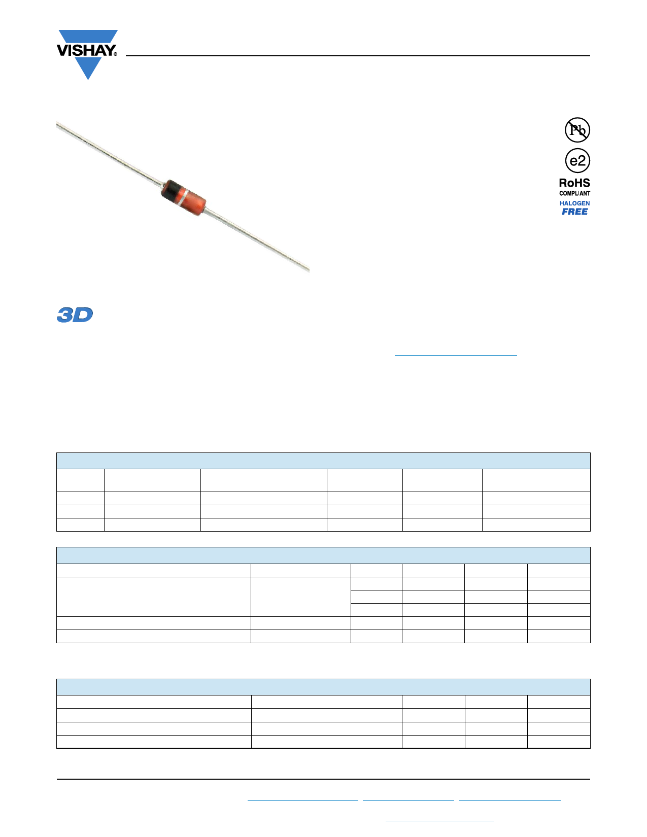
MECHANICAL DATA
Case: DO-35 (DO-204AH)
Weight: approx. 125 mg
Cathode band color: black
Packaging codes/options:
TR/10K per 13" reel (52 mm tape), 50K/box
TAP/10K per ammopack (52 mm tape), 50K/box
PARTS TABLE
PART
TYPE
DIFFERENTIATION
SD103A
SD103B
SD103C
VR = 40 V
VR = 30 V
VR = 20 V
ORDERING CODE
SD103A-TR or SD103A-TAP
SD103B-TR or SD103B-TAP
SD103C-TR or SD103C-TAP
FEATURES
• The SD103 series is a metal-on-silicon Schottky
barrier device which is protected by a PN
junction guardring
• The low forward voltage drop and fast switching
make it ideal for protection of MOS devices,
steering, biasing and coupling diodes for fast
switching and low logic level applications
• Other applications are click suppression,
efficient full wave bridges in telephone subsets, and
blocking diodes in rechargeable low voltage battery
systems
• These diodes are also available in the SOD-123 and
SOD-323 case with type designations SD103AW(S) to
SD103CW(S), and in the MiniMELF case with type
designations LL103A thru LL103C
• For general purpose applications
• AEC-Q101 qualified
• Material categorization: for definitions of compliance
please see www.vishay.com/doc?99912
APPLICATIONS
• HF-detector
• Protection circuit
• Small battery charger
• AC/DC, DC/DC converters
TYPE MARKING
SD103A
SD103B
SD103C
CIRCUIT
CONFIGURATION
Single
Single
Single
REMARKS
Tape and reel/ammopack
Tape and reel/ammopack
Tape and reel/ammopack
ABSOLUTE MAXIMUM RATINGS (Tamb = 25 °C, unless otherwise specified)
PARAMETER
TEST CONDITION
PART
SYMBOL
SD103A
VR
Peak inverse voltage
SD103B
VR
SD103C
VR
Power dissipation (infinite heat sink) (1)
Ptot
Peak forward surge current
tp = 300 μs square pulse
IFSM
Note
(1) Valid provided that leads at a distance of 4 mm from case are kept at ambient temperature
VALUE
40
30
20
400
15
UNIT
V
V
V
mW
A
THERMAL CHARACTERISTICS (Tamb = 25 °C, unless otherwise specified)
PARAMETER
TEST CONDITION
SYMBOL
Thermal resistance junction to ambient air (1)
RthJA
Junction temperature
Tj
Storage temperature range
Tstg
Note
(1) Valid provided that leads at a distance of 4 mm from case are kept at ambient temperature
VALUE
310
125
-55 to +150
UNIT
K/W
°C
°C
Rev. 1.9, 01-Jun-17
1
Document Number: 85754
For technical questions within your region: DiodesAmericas@vishay.com, DiodesAsia@vishay.com, DiodesEurope@vishay.com
THIS DOCUMENT IS SUBJECT TO CHANGE WITHOUT NOTICE. THE PRODUCTS DESCRIBED HEREIN AND THIS DOCUMENT
ARE SUBJECT TO SPECIFIC DISCLAIMERS, SET FORTH AT www.vishay.com/doc?91000
Share Link: 