RFL1P08 Ver la hoja de datos (PDF) - New Jersey Semiconductor
Número de pieza
componentes Descripción
Fabricante
RFL1P08 Datasheet PDF : 2 Pages
| |||
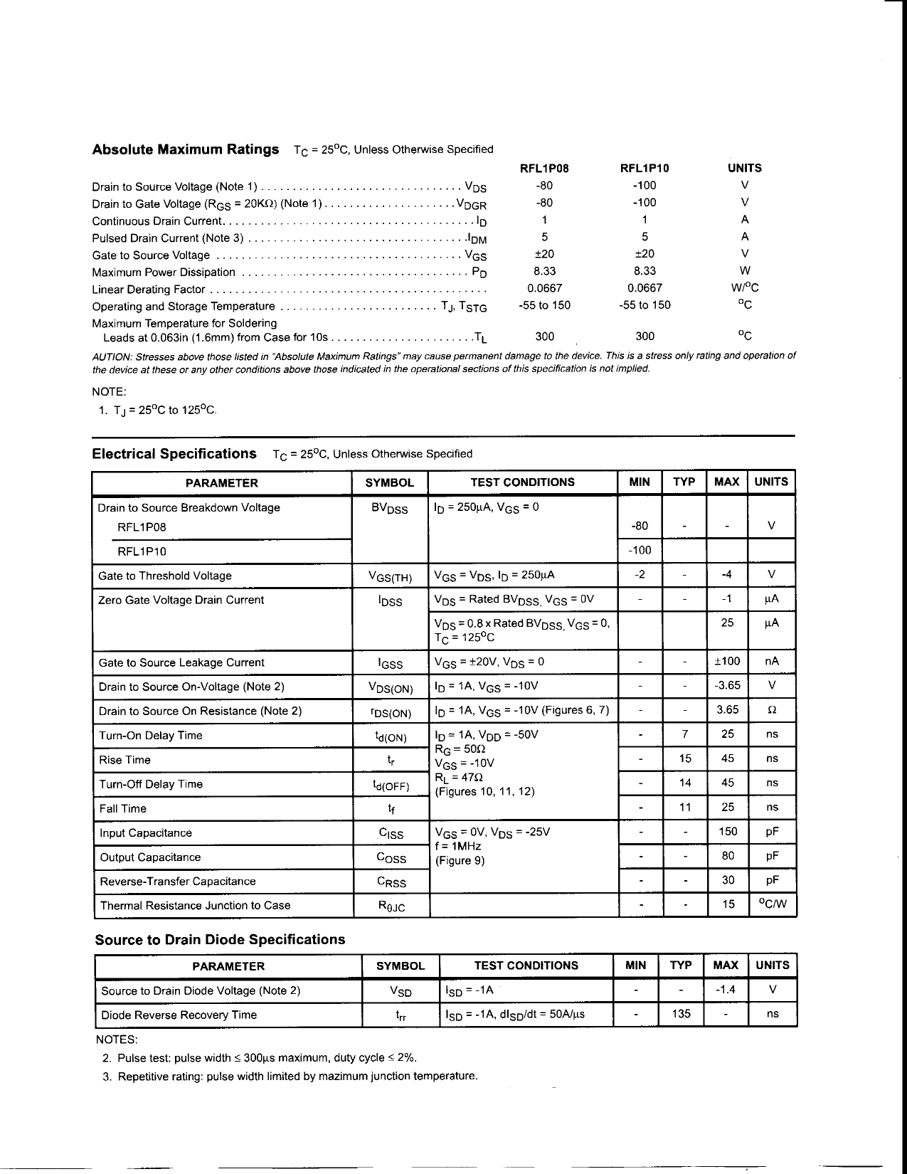
Absolute Maximum Ratings Tc = 25°C, Unless otherwise Specified
Drain to Source Voltage (Note 1 )
Drain to Gate Voltage (RGS = 20KQ) (Note 1 )
.....................
VDGR
Continuous Drain Current
........................................
ID
Pulsed Drain Current (Note 3)
...................................
IDM
Gate to Source Voltage
.......................................
VGs
Maximum Power Dissipation
....................................
PQ
Linear Derating Factor
............................................
Operating and Storage Temperature
.........................
Tj, TSTG
Maximum Temperature for Soldering
Leads at0.063in (1.6mm) from Case for 10s
.......................
T|_
RFL1P08
-80
-80
1
5
±20
8.33
0.0667
-55 to 150
300
RFL1P10
-100
-100
1
5
±20
8.33
0.0667
-55 to 150
300
UNITS
V
V
A
A
V
W
W/°C
°C
AUTION: Stresses above those listed in "Absolute Maximum Ratings" may cause permanent damage to the device. This is a stress only rating and operation of
the device at these or any other conditions above those indicated in the operational sections of this specification is not implied.
NOTE:
= 25°Cto125°C.
Electrical Specifications Tc = 25°C, Unless Otherwise Specified
PARAMETER
Drain to Source Breakdown Voltage
RFL1P08
RFL1P10
Gate to Threshold Voltage
Zero Gate Voltage Drain Current
Gate to Source Leakage Current
Drain to Source On-Voltage (Note 2)
Drain to Source On Resistance (Note 2)
Turn-On Delay Time
Rise Time
Turn-Off Delay Time
Fall Time
Input Capacitance
Output Capacitance
Reverse-Transfer Capacitance
Thermal Resistance Junction to Case
SYMBOL
TEST CONDITIONS
MIN
BVDSS ID = 250nA, VGS = o
-80
-100
VGS(TH) VGS = VDS, ID = 250|j.A
-2
'DSS
VDS = Rated BVDSs, VGS = ov
-
VDS = 0.8 x Rated BVDSS VGS = 0,
TC=125°C
'GSS ves = ±2ov, VDS =o
-
VDS(ON) ID = 1A, VGS = -10V
-
rDS(ON) ID = 1A> VGS = -10V (Figures e, 7) -
td(ON)
ID=1A,VDD = -50V
-
RG — 50£1
tr
VGS = -10V
-
'd(OFF)
RL = 47Q
(Figures 10, 11, 12)
-
tf
-
CISS
VGS = OV, VDS =-25V
-
coss
(Figure 9)
-
CRSS
-
R9JC
-
TYP MAX UNITS
_
_
V
-
-4
V
-
-1
^A
25
HA
-
±100
nA
- -3.65
V
-
3.65
n
7
25
ns
15
45
ns
14
45
ns
11
25
ns
-
150
PF
-
80
PF
-
30
pF
-
15 °C/W
Source to Drain Diode Specifications
PARAMETER
SYMBOL
TEST CONDITIONS
Source to Drain Diode Voltage (Note 2)
VSD
ISD = -1A
Diode Reverse Recovery Time
trr
ISD = -1A, dlSD/dt = SOA/ns
NOTES:
2. Pulse test: pulse width < 300|is maximum, duty cycle < 2%.
3. Repetitive rating: pulse width limited by mazimum junction temperature.
MIN TYP MAX UNITS
-
-
-1.4
V
-
135
-
ns
Share Link: 