CS2841B(2008) Ver la hoja de datos (PDF) - ON Semiconductor
Número de pieza
componentes Descripción
Fabricante
CS2841B Datasheet PDF : 10 Pages
| |||
CS2841B
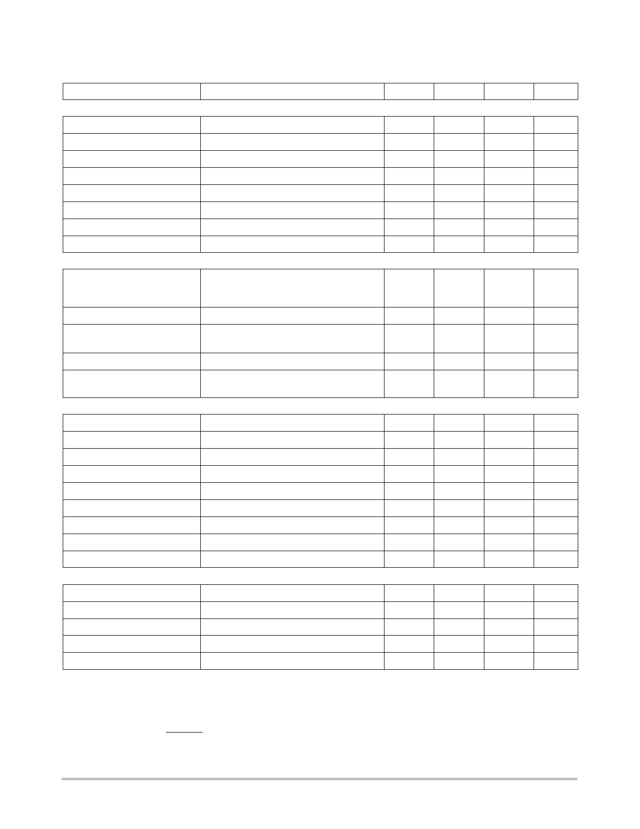
ELECTRICAL CHARACTERISTICS (-40°C ≤ TA ≤ 85°C, RT = 680 kW, CT = 0.022 mF for Triangular Mode, VCC = 15 V (Note 3),
RT = 10 kW, CT = 3.3 nF for Sawtooth Mode (see Figure 7); unless otherwise specified.)
Characteristic
Test Conditions
Min
Typ
Max
Unit
Reference Section
Output Voltage
Line Regulation
Load Regulation
Temperature Stability
TJ = 25°C, IOUT = 1.0 mA
8.4 ≤ VCC ≤ 16 V
1.0 ≤ IOUT ≤ 20 mA
Note 4
4.9
5.0
5.1
V
-
6.0
20
mV
-
6.0
25
mV
-
0.2
0.4
mV/°C
Total Output Variation
Line, Load, Temp. Note 4
4.82
-
5.18
V
Output Noise Voltage
Long Term Stability
Output Short Circuit
Oscillator Section
10 Hz ≤ f ≤ 10 kHz, TJ = 25°C. Note 4
TA = 125°C, 1000 Hrs. Note 4
TA = 25°C
-
50
-
mV
-
5.0
25
mV
-30
-100
-180
mA
Initial Accuracy
Voltage Stability
Temperature Stability
Amplitude
Discharge Current
Error Amp Section
Sawtooth Mode: TJ = 25°C. See Figure 7.
47
52
57
kHz
Sawtooth Mode: -40°C ≤ TA ≤ +85°C
44
52
60
kHz
Triangular Mode: TJ =25°C. See Figure 7.
44
52
60
kHz
8.4 ≤ VCC ≤ 16 V
-
0.2
1.0
%
Sawtooth Mode: TMIN ≤ TA ≤ TMAX. Note 4
-
5.0
-
%
Triangular Mode: TMIN ≤ TA ≤ TMAX. Note 4
-
8.0
-
%
VOSC (Peak to Peak)
-
1.7
-
V
TJ = 25°C
TMIN ≤ TA ≤ TMAX
7.4
8.3
9.2
mA
7.2
-
9.4
mA
Input Voltage
Input Bias Current
AVOL
Unity Gain Bandwidth
VCOMP = 2.5 V
VFB = 0 V
2.0 ≤ VOUT ≤ 4.0 V
Note 4
2.42
2.5
2.58
V
-
-0.3
-2.0
mA
65
90
-
dB
0.7
1.0
-
MHz
PSRR
Output Sink Current
Output Source Current
VOUT High
VOUT Low
Current Sense Section
8.4 V ≤ VCC ≤ 16 V
VFB = 2.7 V, VCOMP = 1.1 V
VFB = 2.3 V, VCOMP = 5.0 V
VFB = 2.3 V, RL = 15 kW to Ground
VFB = 2.7 V, RL = 15 kW to VREF
60
70
-
dB
2.0
6.0
-
mA
-0.5
-0.8
-
mA
5.0
6.0
-
V
-
0.7
1.1
V
Gain
Notes 5 and 6
2.85
3.0
3.15
V/V
Maximum Input Signal
VCOMP = 5.0 V. Note 5
PSRR
12 V ≤ VCC ≤ 25 V. Note 5
Input Bias Current
VSense = 0 V
Delay to Output
TJ = 25°C. Note 4
3. Adjust VCC above the start threshold before setting at 15 V
4. These parameters, although guaranteed, are not 100% tested in production
5. Parameter measured at trip point of latch with VFB = 0
6. Gain defined as:
0.9
1.0
1.1
V
-
70
-
dB
-
-2.0
-10
mA
-
150
300
ns
A
+
DVCOMP
DVSense
;Ă
0
v
VSense
v
0.8ĂV.
http://onsemi.com
3
Share Link: 