SLVU2.8-8(2007) Ver la hoja de datos (PDF) - ProTek Devices.
Número de pieza
componentes Descripción
Fabricante
SLVU2.8-8 Datasheet PDF : 5 Pages
| |||
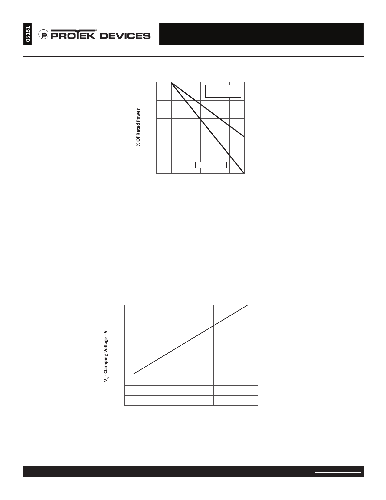
SLVU2.8-8
APPLICATION NOTE
Electronic equipment is susceptible to damage caused by Electrostatic Discharge (ESD), Electrical Fast Transients (EFT), and tertiary lightning effects.
Knowing that equipment can be damaged, the SLVU2.8-8 was designed to provide the level of protection required to safe guard sensitive equipment.
This product can be used in different configurations to provide a level of protection to meet bidirectional requirements either in a common-mode or
differential-mode configuration.
BIDIRECTIONAL COMMON-MODE CONFIGURATION (Figure 1)
The SLVU2.8-8 provides up to four lines of protection in a common-mode configuration as
depicted in figure 1.
Figure 1. Bidirectional Common-Mode Protection
Circuit connectivity is as follows:
✔ Line 1 is connected to Pin 1
✔ Line 2 is connected to Pin 8
✔ Line 3 is connected to Pin 5
✔ Line 4 is connected to Pin 4
✔ Pins 2, 3, 6 and 7 are connected to ground
BIDIRECTIONAL DIFFERENTIAL-MODE CONFIGURATION (Figure 2)
The SLVU2.8-8 provides up to four line paris of protection in a differential-mode configura-
tion as depicted in figure 2.
Circuit connectivity is as follows:
✔ Line Pair 1 is connected to Pins 1 & 2
✔ Line Pair 2 is connected to Pins 3 & 4
✔ Line Pair 3 is connected to Pins 7 & 8
✔ Line Pair 4 is connected to Pins 5 & 6
CIRCUIT BOARD LAYOUT RECOMMENDATIONS
Circuit board layout is critical for Electromagnetic
Compatibility (EMC) protection. The following
guidelines are recommended:
✔ The protection device should be placed near the
input terminals or connectors, the device will
divert the transient current immediately before it
can be coupled into the nearby traces.
✔ The path length between the TVS device and
the protected line should be minimized.
✔ All conductive loops including power and ground
loops should be minimized.
✔ The transient current return path to ground
should be kept as short as possible to reduce
parasitic inductance.
✔ Ground planes should be used whenever
possible. For multilayer PCBs, use ground vias.
Figure 2. Bidirectional Differential-Mode Protection
05181.R3 3/07
4
www.protekdevices.com
Share Link: 