TNY289KG Ver la hoja de datos (PDF) - Power Integrations, Inc
Número de pieza
componentes Descripción
Fabricante
TNY289KG
Power Integrations, Inc

TNY289KG Datasheet PDF : 26 Pages
| |||
TNY284-290
a Zener diode across the DC output voltage to be regulated.
When the output voltage exceeds the target regulation voltage
level (optocoupler LED voltage drop plus Zener voltage), the
optocoupler LED will start to conduct, pulling the ENABLE/
UNDERVOLTAGE pin low. The Zener diode can be replaced by
a TL431 reference circuit for improved accuracy.
ON/OFF Operation with Current Limit State Machine
The internal clock of the TinySwitch-4 runs all the time. At the
beginning of each clock cycle, it samples the ENABLE/
UNDERVOLTAGE pin to decide whether or not to implement a
switch cycle, and based on the sequence of samples over
multiple cycles, it determines the appropriate current limit. At
high loads, the state machine sets the current limit to its highest
value. At lighter loads, the state machine sets the current limit
to reduced values.
At near maximum load, TinySwitch-4 will conduct during nearly
all of its clock cycles (Figure 7). At slightly lower load, it will
“skip” additional cycles in order to maintain voltage regulation at
the power supply output (Figure 8). At medium loads, cycles
will be skipped and the current limit will be reduced (Figure 9).
At very light loads, the current limit will be reduced even further
(Figure 10). Only a small percentage of cycles will occur to
satisfy the power consumption of the power supply.
The response time of the ON/OFF control scheme is very fast
compared to PWM control. This provides tight regulation and
excellent transient response.
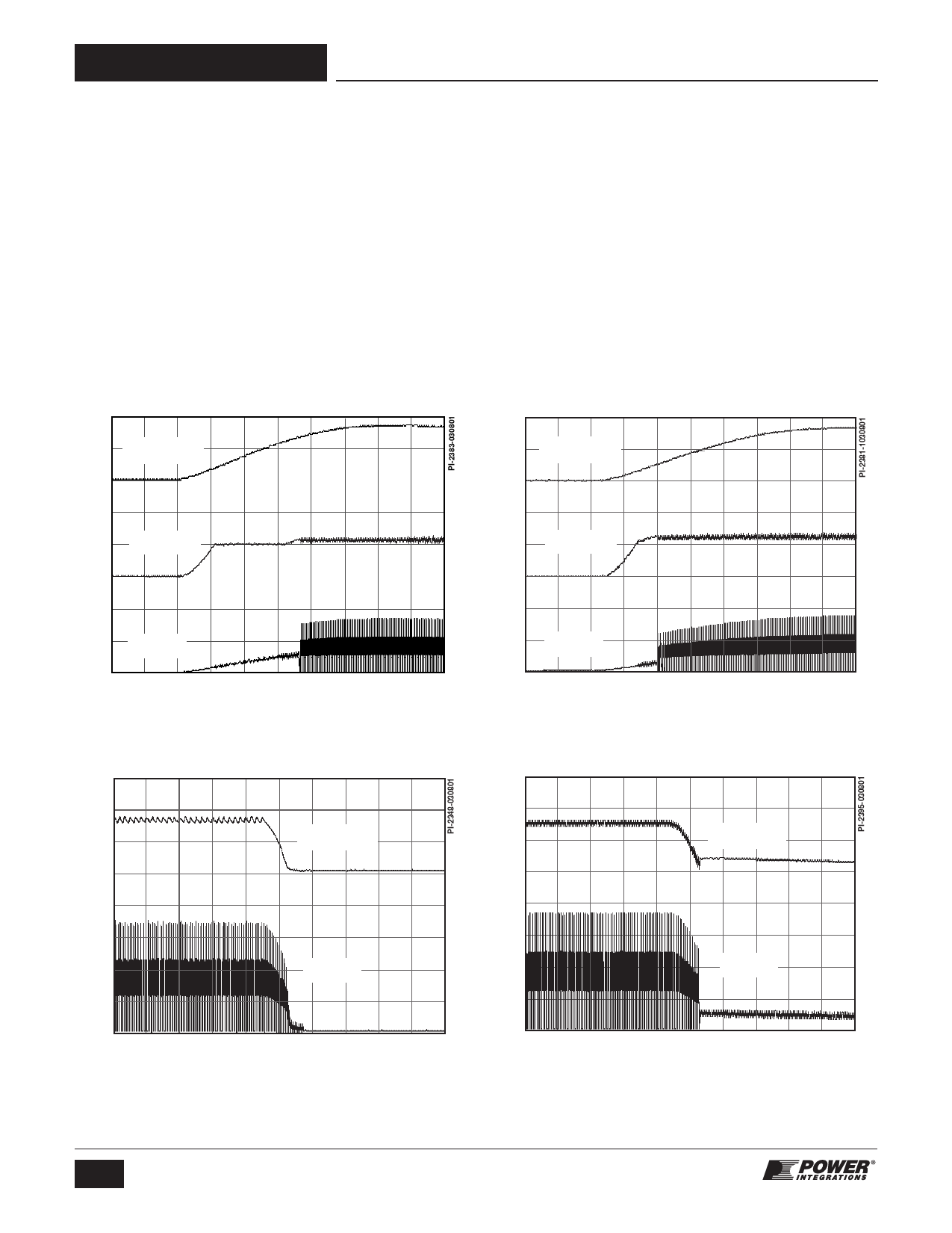
Power-Up/Down
The TinySwitch-4 requires only a 0.1 μF capacitor on the
BYPASS/MULTI-FUNCTION pin to operate with standard
200
100
V
DC-INPUT
0
10
5
V
BYPASS
0
400
200
V
DRAIN
0
0
1
2
Time (ms)
Figure 11. Power-Up with Optional External UV Resistor (4 MW)
Connected to EN/UV Pin.
200
100
V
DC-INPUT
0
10
5
V
BYPASS
0
400
200
V
DRAIN
0
0
1
2
Time (ms)
Figure 12. Power-Up without Optional External UV Resistor
Connected to EN/UV Pin.
200
V
100
DC-INPUT
0
400
300
200
V
DRAIN
100
0
0
.5
Time (s)
Figure 13. Normal Power-Down Timing (without UV).
200
100
V
DC-INPUT
0
400
300
200
V
DRAIN
100
0
1
0
2.5
5
Time (s)
Figure 14. Slow Power-Down Timing with Optional External (4 MW)
UV Resistor Connected to EN/UV Pin.
6
Rev. A 09/12
www.powerint.com
Share Link: