CDS-1401MM-C Ver la hoja de datos (PDF) - DATEL Data Acquisition products
Número de pieza
componentes Descripción
Fabricante
CDS-1401MM-C
DATEL Data Acquisition products

CDS-1401MM-C Datasheet PDF : 1 Pages
| |||
FEATURES
Use with 10 to 14-bit A/D converters
1.25 Megapixels/second minimum throughput
(14 bits)
±10V input/output ranges, Gain = –1
Low noise, 200μVrms
Two independent S/H amplifiers
Gain matching between S/H's
Offset adjustments for each S/H
Four external A/D control lines
Small package, 24-pin ceramic DDIP
Low power, 700mW
Low cost
CDS-1401
14-Bit, Fast-Settling Correlated Double Sampling Circuit
PRODUCT OVERVIEW
The CDS-1401 is an application-specific, cor-
related double sampling (CDS) circuit designed for
electronic-imaging applications that employ CCD’s
(charge coupled devices) as their photodetec-
tor. The CDS-1401 has been optimized for use in
digital video applications that employ 10 to 14-bit
A/D converters. The low-noise CDS-1401 can
accurately determine each pixel’s true video signal
level by sequentially sampling the pixel’s offset
signal and its video signal and subtracting the two.
The result is that the consequences of residual
charge, charge injection and low-frequency “kTC”
noise on the CCD’s output floating capacitor are
effectively eliminated. The CDS-1401 can also be
used as a dual sample-hold amplifier in a data
acquisition system.
The CDS-1401 contains two sample-hold
amplifiers and appropriate support/control circuitry.
Features include independent offset-adjust capabil-
ity for each S/H, adjustment for matching gain
between the two S/H’s, and four control lines for
triggering the A/D converter used in conjunction
with the CDS-1401. The CDS circuit’s “ping-pong”
timing approach (the offset signal of the “n+1”
pixel can be acquired while the video output of
the “nth” pixel is being converted) guarantees a
minimum throughput, in a 14-bit application, of
1.25MHz. In other words, the true video signal
(minus offset) will be available at the output of the
CDS-1401 every 800ns. This correlates with the
fact that an acquisition time of 400ns is required
for each internal S/H amplifier (10V step setting to
±0.003%). The input and output of the CDS-1401
can swing up to ±10 Volts.
The functionally complete CDS-1401 is pack-
aged in a single, 24-pin, ceramic DDIP. It oper-
ates from ±15V and +5V supplies and consumes
700mW. Though the CDS-1401’s approach to
CDS appears straightforward (see Description of
Operation), the circuit actually exploits an elegant
architecture whose tradeoffs enable it to offer
wide-bandwidth, low-noise and highthrough-
put combinations unachievable until now. The
CDS- 1401 is a generic type of circuit that can be
used with almost any 10 to 14-bit A/D converter.
However, DATEL does offer A/D converters that are
optimized for use with the CDS-1401.
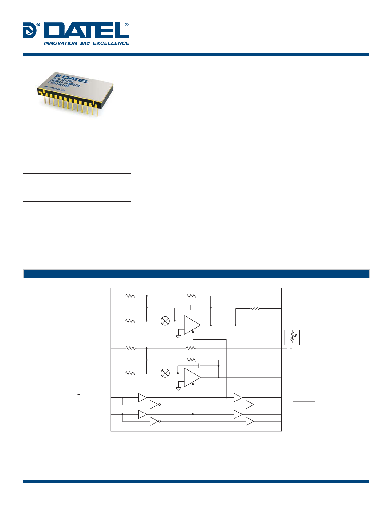
BLOCK DIAGRAM
OFFSET ADJUST V1 1
OFFSET ADJUST I1 2
ANALOG INPUT 1 3
100k7
1k7
OFFSET ADJUST V2 9
OFFSET ADJUST I2 10
ANALOG INPUT 2 4
100k7
1k7
1k7
CH = 100pF
–
S/H 1
+
9007
1k7
– CH = 100pF
S/H 2
+
1007
7 S/H1 ROUT
6 S/H1 OUT
OPTIONAL
8 S/H2
SUMMING NODE
22 V OUT
S/H1 COMMAND 11
S/H2 COMMAND 12
18 A/D CLOCK 1
17 A/D CLOCK 1
19 A/D CLOCK 2
20 A/D CLOCK 2
5, 14, 21, 23
ANALOG GROUND
24
+15V SUPPLY
13
–15V SUPPLY
16
+5V DIGITAL
SUPPLY
Figure 1. CDS-1401 Functional Block Diagram
15
DIGITAL
GROUND
DATEL, Inc. 11 Cabot Boulevard, Mansfield, MA 02048-1151 USA • Tel: (508) 339-3000 • www.datel.com • e-mail: help@datel.com
06 Oct 2015 MDA_CDS-1401.B03 Page 1 of 9
Share Link: