DU1P0-05S05 Ver la hoja de datos (PDF) - Power Mate Technology
Número de pieza
componentes Descripción
Fabricante
DU1P0-05S05 Datasheet PDF : 2 Pages
| |||
DU1P0 SERIES
1 WATTS DC-DC CONVERTER
Model
Number
DU1P0-05S05
DU1P0-05S12
DU1P0-05S15
DU1P0-05D05
DU1P0-05D12
DU1P0-05D15
DU1P0-12S05
DU1P0-12S12
DU1P0-12S15
DU1P0-12D05
DU1P0-12D12
DU1P0-12D15
DU1P0-15S05
DU1P0-15S12
DU1P0-15S15
DU1P0-15D05
DU1P0-15D12
DU1P0-15D15
DU1P0-24S05
DU1P0-24S12
DU1P0-24S15
DU1P0-24D05
DU1P0-24D12
DU1P0-24D15
Input
Range
4.5 ~ 5.5 VDC
4.5 ~ 5.5 VDC
4.5 ~ 5.5 VDC
4.5 ~ 5.5 VDC
4.5 ~ 5.5 VDC
4.5 ~ 5.5 VDC
10.8 ~ 13.2 VDC
10.8 ~ 13.2 VDC
10.8 ~ 13.2 VDC
10.8 ~ 13.2 VDC
10.8 ~ 13.2 VDC
10.8 ~ 13.2 VDC
13.5 ~ 16.5 VDC
13.5 ~ 16.5 VDC
13.5 ~ 16.5 VDC
13.5 ~ 16.5 VDC
13.5 ~ 16.5 VDC
13.5 ~ 16.5 VDC
21.6 ~ 26.4 VDC
21.6 ~ 26.4 VDC
21.6 ~ 26.4 VDC
21.6 ~ 26.4 VDC
21.6 ~ 26.4 VDC
21.6 ~ 26.4 VDC
Output
Voltage
5 VDC
12 VDC
15 VDC
± 5 VDC
± 12 VDC
± 15 VDC
5 VDC
12 VDC
15 VDC
± 5 VDC
± 12 VDC
± 15 VDC
5 VDC
12 VDC
15 VDC
± 5 VDC
± 12 VDC
± 15 VDC
5 VDC
12 VDC
15 VDC
± 5 VDC
± 12 VDC
± 15 VDC
Output Current
Output (3)
No load(2)
Min. load Full load Ripple & Noise Input Current
20mA
8.3mA
6.7mA
± 10mA
± 4.2mA
± 3.3mA
20mA
8.3mA
6.7mA
± 10mA
± 4.2mA
± 3.3mA
20mA
8.3mA
6.7mA
± 10mA
± 4.2mA
± 3.3mA
20mA
8.3mA
6.7mA
± 10mA
± 4.2mA
± 3.3mA
200mA
83mA
67mA
± 100mA
± 42mA
± 33mA
200mA
83mA
67mA
± 100mA
± 42mA
± 33mA
200mA
83mA
67mA
± 100mA
± 42mA
± 33mA
200mA
83mA
67mA
± 100mA
± 42mA
± 33mA
100mVp-p
100mVp-p
100mVp-p
100mVp-p
100mVp-p
100mVp-p
100mVp-p
100mVp-p
100mVp-p
100mVp-p
100mVp-p
100mVp-p
100mVp-p
100mVp-p
100mVp-p
100mVp-p
100mVp-p
100mVp-p
100mVp-p
100mVp-p
100mVp-p
100mVp-p
100mVp-p
100mVp-p
42mA
32mA
35mA
40mA
35mA
40mA
17mA
17mA
18mA
18mA
18mA
18mA
20mA
18mA
18mA
18mA
16mA
16mA
12mA
12mA
10mA
12mA
10mA
10mA
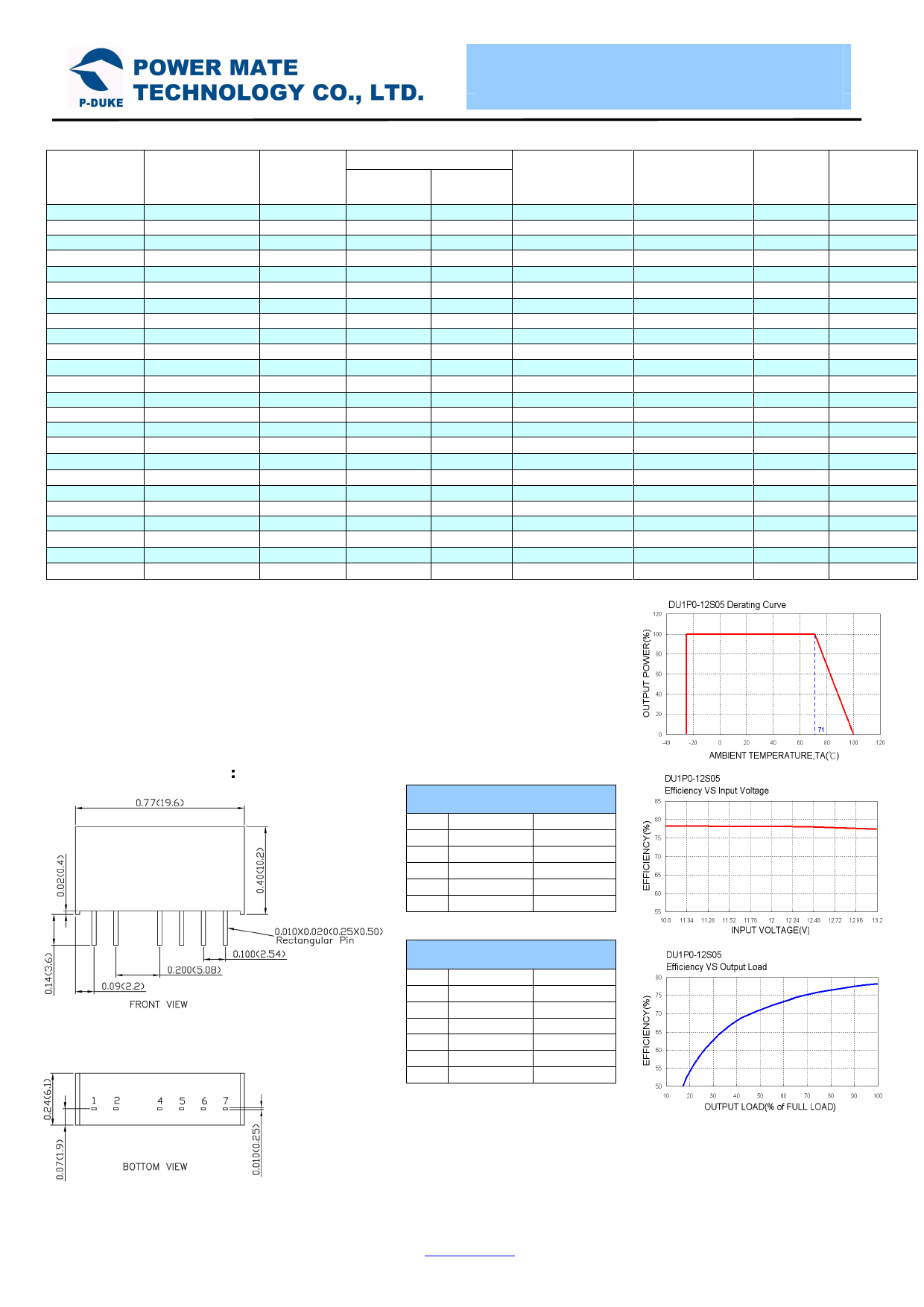
Note
1. MIL-HDBK-217F @Ta=25 ºC, Full load.
2. Typical value at nominal input voltage and no load.
3. Typical value at nominal input voltage and full load.
4. Test by minimum Vin and constant resistive load.
5. The output requires a minimum loading on the output to maintain specified regulation.
Operation under no-load condition will not damage these devices, however they may not meet all
listed specification.
CAUTION: This power module is not internally fused. An input line fuse must always be used.
: MECHANICAL DRAWING
STANDARD
PIN SINGLE
DUAL
1
+INPUT
+INPUT
2
-INPUT
-INPUT
4 -OUTPUT -OUTPUT
5
NC
COMMON
6 +OUTPUT +OUTPUT
Eff (3)
(%)
77
82
81
78
82
81
77
82
79
77
81
82
73
79
80
75
80
80
72
78
78
75
78
79
Capacitor
Load
max(4)
330µF
330µF
330µF
±150µF
±150µF
±150µF
330µF
330µF
330µF
±150µF
±150µF
±150µF
330µF
330µF
330µF
±150µF
±150µF
±150µF
330µF
330µF
330µF
±150µF
±150µF
±150µF
“SUFFIX-N” Models
PIN SINGLE
1
+INPUT
2
-INPUT
DUAL
+INPUT
-INPUT
5 -OUTPUT -OUTPUT
6
NC
COMMON
7 +OUTPUT +OUTPUT
1. All dimensions in Inch (mm)
Tolerance: X.XX±0.02 (X.X±0.5)
X.XXX±0.01 (X.XX±0.25)
2. Pin pitch tolerance ±0.01 (0.25)
3. Pin dimension tolerance ±0.004 (0.1)
Page 2 of 2
www.pduke.com
2014/4/30
Share Link: 