DMC42C1106 Ver la hoja de datos (PDF) - Daewoo Semiconductor
Número de pieza
componentes Descripción
Fabricante
DMC42C1106 Datasheet PDF : 20 Pages
| |||
4Bit Single Chip Microcontroller
7
DMC42C1106
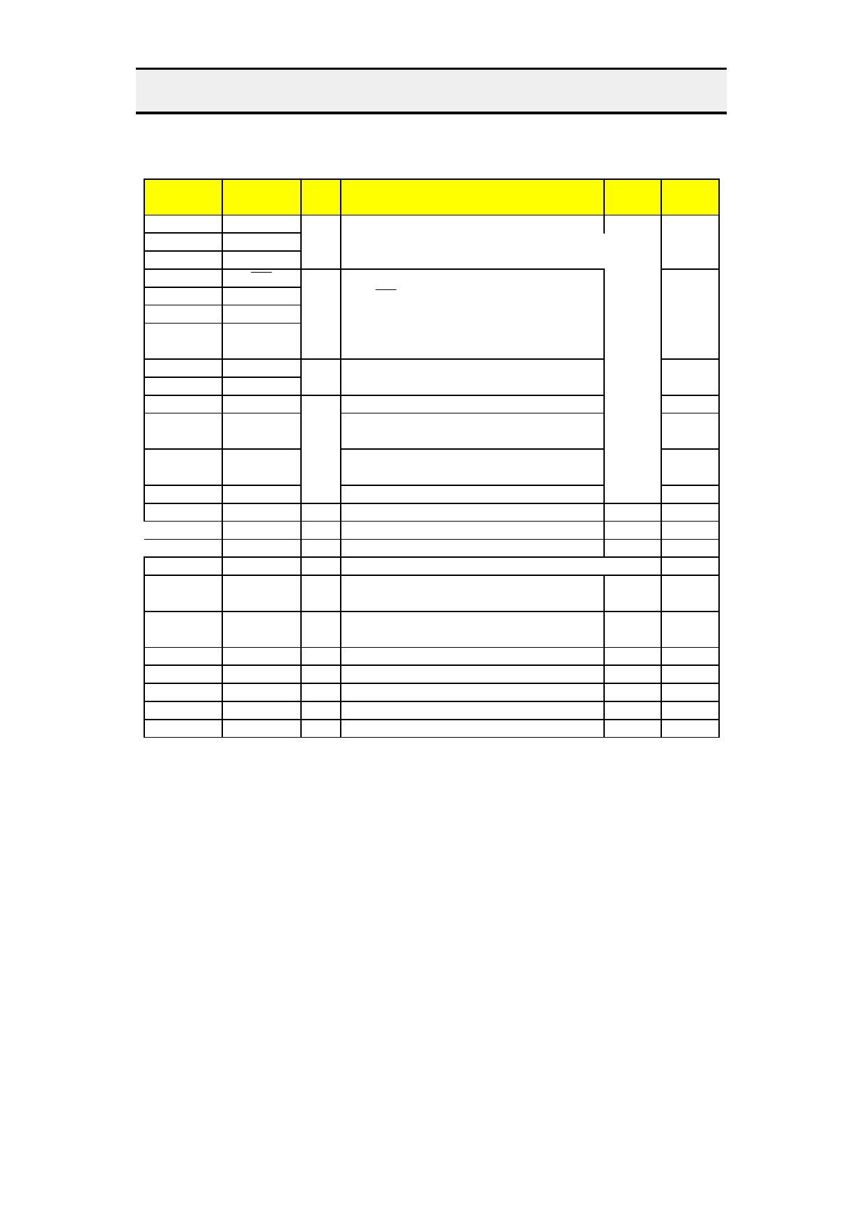
PIN DESCRIPTION
PIN
SYMBOL
P00
P01
P02
P10
P11
P12
P13
SHARED
PIN
INT0/TI0
INT1/TI1
INT2
SCK
SI
SO
BUZ
P20
P21 ~ P23
P40 ~ P43
PA0 ~ PA3
CLO
-
-
AD0~AD3
PB0 ~ PB3 AD4~AD7
PC2 ~ PC3
-
VLC0~VLC2
-
COM0~COM3
-
SEG0~SEG19
-
SEG20
-
XI
-
XO
XTI
-
XTO
RESETB
-
TEST
-
DGRMEN
-
AVDD,
-
VDD, VSS
-
I/O
FUNCTION
RESET PORT
TYPE
- 3 bit I/O Port (PORT0)
I/O - INT0, 1, 2 pins are the external interrupt inputs
BPS
- TI0, 1 pins are the timer/event counter inputs
- 4 bit I/O Port (PORT1)
- The SCK pin is the serial clock input
I/O - The SI pin is the serial data input
BPS
- The SO pin is the serial data output
- The BUZ pin is the watch timer signal output INPUT
I/O - 4 bit I/O Port (PORT2)
BPS
- The CLO pin is the system clock output
BP
4 bit I/O Port (PORT4)
BDR
- 4 bit I/O Port (PORTA)
BPA
I/O - Analog input port
- 4 bit I/O Port (PORTB)
BPA
- Analog input port
2 bit I/O Port
BDR
I LCD bias inputs
O LCD common signal outputs
OCOM
O LCD segment signal outputs
OSEG-A
O LCD segment signal output and 1 bit data output
OSEG-B
- XI, XO are main oscillator input pin, output
OSC1
pin, respectively
- XTI, XTO are sub oscillator input, output
OSC2
pin respectively
I Reset input pin
IP1
- No connection ( must be connect to VSS )
IP2
- No connection
- Power & ground for the A/D convertor
- Power & ground
Share Link: 