74LVC27BQ Ver la hoja de datos (PDF) - NXP Semiconductors.
Número de pieza
componentes Descripción
Fabricante
74LVC27BQ Datasheet PDF : 14 Pages
| |||
NXP Semiconductors
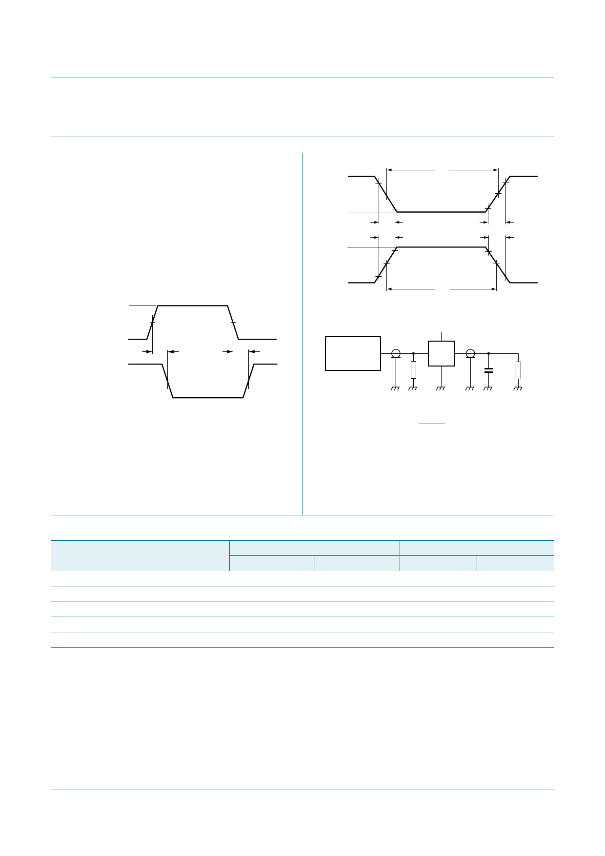
11. AC waveforms
74LVC27
Triple 3-input NOR gate
VI
nA, nB, nC
input
GND
VOH
nY output
VOL
VM
t PHL
VM
t PLH
mna938
VM = 1.5 V at VCC 2.7 V
VM = 0.5 VCC at VCC < 2.7 V.
VOL and VOH are typical output voltage levels that occur
with the output load.
Fig 6. Input (nA, nB and nC) to output (nY)
propagation delays
tW
VI 90 %
negative
pulse
VM
10 %
0V
tf
VI
positive
pulse
tr
90 %
VM
10 %
0V
tW
VM
tr
tf
VM
VCC
VI
PULSE
GENERATOR
VO
DUT
RT
CL
RL
001aaf615
Fig 7.
Test data is given in Table 8. Definitions for test circuit:
RL = Load resistance.
CL = Load capacitance including jig and probe
capacitance.
RT = Termination resistance should be equal to output
impedance Zo of the pulse generator.
Test circuit for measuring switching times
Table 8. Test data
Supply voltage
1.2 V
1.65 V to 1.95 V
2.3 V to 2.7 V
2.7 V
3.0 V to 3.6 V
Input
VI
VCC
VCC
VCC
2.7 V
2.7 V
tr, tf
2 ns
2 ns
2 ns
2.5 ns
2.5 ns
Load
CL
30 pF
30 pF
30 pF
50 pF
50 pF
RL
1 k
1 k
500
500
500
74LVC27
Product data sheet
All information provided in this document is subject to legal disclaimers.
Rev. 6 — 27 October 2011
© NXP B.V. 2011. All rights reserved.
6 of 14
Share Link: 