CXD3605R Ver la hoja de datos (PDF) - Sony Semiconductor
Número de pieza
componentes Descripción
Fabricante
CXD3605R Datasheet PDF : 36 Pages
| |||
CXD3605R
Control data: D32 FGOB [Wide OBCLP generation]
This controls wide OBCLP generation during the vertical OPB period. See the Timing Charts for the actual
operation. The default is "OFF".
D32
Description of operation
0 Wide OBCLP generation OFF
1 Wide OBCLP generation ON
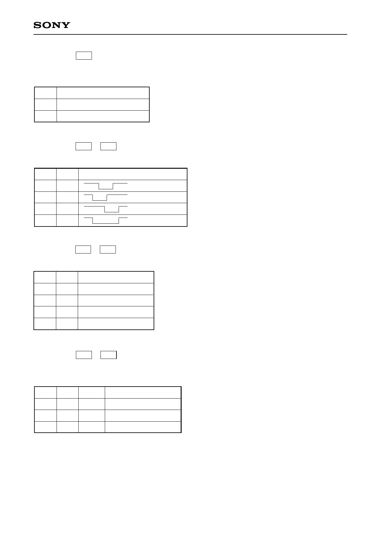
Control data: D34 to D35 PTOB [OBCLP waveform pattern]
This indicates the OBCLP waveform pattern. The default is "Normal".
D35 D34
0
0
0
1
1
0
1
1
Waveform pattern
(Normal)
(Shifted rearward)
(Shifted forward)
(Wide)
Control data: D36 to D37 LOAD [ADCLK logical phase]
This indicates the ADCLK logic phase adjustment data. The default is 90° relative to MCKO.
D37 D36 Degree of adjustment (°)
0
0
0
0
1
90
1
0
180
1
1
270
Control data: D38 to D39 STB [Standby]
The operating mode is switched as follows. However, the standby bits are loaded to the CXD3605R and
control is applied immediately at the rising edge of SEN.
D39 D38 Symbol
Operating mode
X
0 CAM Normal operating mode
0
1 SLP Sleep mode
1
1 STB Standby mode
See the Pin Status Table for the pin status in each mode.
– 18 –
Share Link: 