CXD3605R Ver la hoja de datos (PDF) - Sony Semiconductor
Número de pieza
componentes Descripción
Fabricante
CXD3605R Datasheet PDF : 36 Pages
| |||
CXD3605R
[HTSG control mode]
This mode controls the V1A/B and V3A/B ternary level outputs (readout pulse block) using D14 HTSG.
D14
Description of operation
0 Readout pulse (SG) normal operation
1 HTSG control mode
VD
V1A
SUB
Vck
WEN
EXP
HTSG
0
SMD
1
Exposure time
1
0
0
1
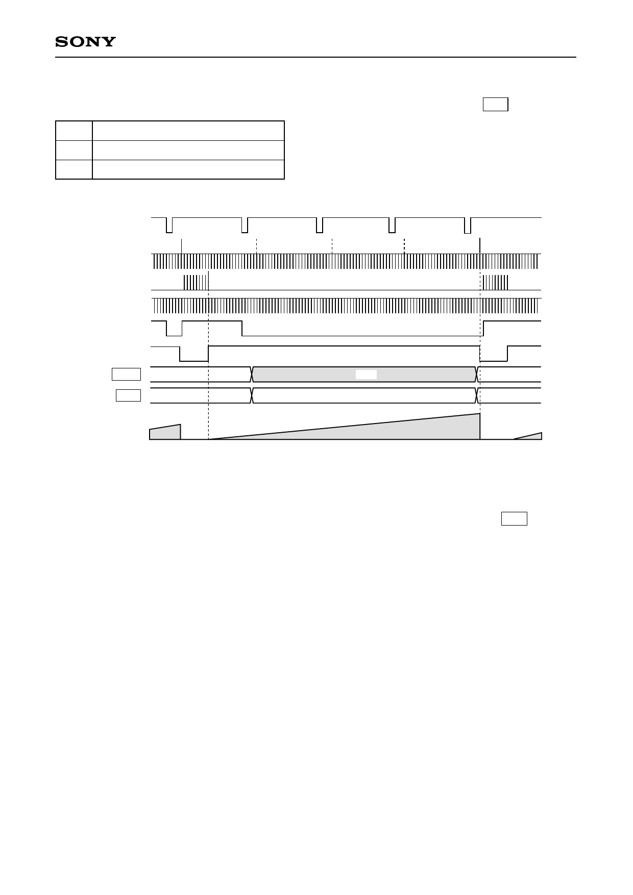
[EXP pulse]
The ID/EXP pin (Pin 4) output can be switched between the ID pulse or the EXP pulse using D33 EXP. The
default is the "ID" pulse. See the Timing Charts for the ID pulse. The EXP pulse indicates the exposure time
when it is high. The transition point is the last SUB pulse falling edge, and midpoint value (1338ck) of each
V1A/B and V3A/B ternary out put falling edge. When there is no SUB pulse, the later ternary output falling
edge (1416ck) is used. See the EXP pulse indicated in the explanatory diagrams under [Electronic shutter] for
an image of operation.
Note that the above specification is based on draft mode. For frame mode, the former value is 1260ck and the
latter value is 1416ck.
– 21 –
Share Link: 