CMPWR280 Ver la hoja de datos (PDF) - California Micro Devices => Onsemi
Número de pieza
componentes Descripción
Fabricante
CMPWR280 Datasheet PDF : 10 Pages
| |||
CALIFORNIA MICRO DEVICES
CMPWR280
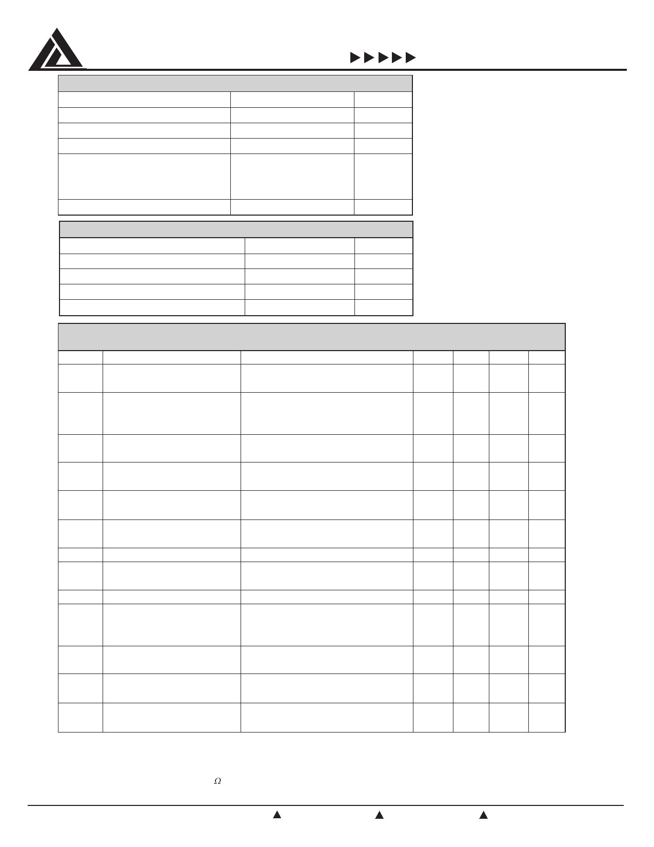
ABSOLUTE MAXIMUM RATINGS
Parameter
Rating
ESD Protection (HBM)
2000
VCC , VSBY , VOUT
Drive Logic Voltage
Storage Temperature Range
+6.0, Gnd -0.5
VCC (VSBY) +0.5, GND -0.5
-40 to +150
Operating Ambient
0 to +70
Operating Junction
0 to +150
Power Dissipation: (TO-263) Note 1
Internally Limited
Unit
V
V
V
oC
W
OPERATING CONDITIONS
Parameter
Range
VCC, VSBY
Temperature (Ambient)
5.0 ± 0.25
0 to +70
Load Current
0 to 1500
C EXT
10 ± 10%
Unit
V
oC
mA
µF
ELECTRICAL OPERATING CHARACTERISTICS
(over operating conditions unless specified otherwise)
Symbol Parameter
Conditions
MIN TYP MAX UNIT
V OUT
Regulator Output Voltage
0mA < ILOAD < 1500mA (VCC )
3.135 3.30 3.465 V
0mA < ILOAD < 375mA (VSBY )
V CCSEL
Select Voltage
VCC Regulator Enabled
4.50 4.70
VCCDES VCC Deselect Voltage
VCC Regulator Disabled
3.90 4.10
V
VCCHYST Hysteresis Voltage
VCC Hysteresis: Note 2
0.40
IOUT
Maximum Output Current
VCC selected
1500 2500
mA
VSBY selected
375 750
IS/C
Short Circuit Output Current VCC selected
800
mA
VSBY selected
200
IRCC
VCC Pin Reverse Leakage
VCC = 0V. VSBY = 5V
10
100
µA
IRSBY
VSBY Pin Reverse Leakage
VSBY = 0V. VCC = 5V
10
10
VR LOAD VCC Load Regulation
VCC selected, ILOAD = 15mA to 1500mA
30
mV
VSBY Load Regulation
VSBY selected, ILOAD = 5mA to 375mA
30
VR LINE
Line Regulation
VCC = 4.5V to 5.5V, ILOAD = 5mA
5
mV
ICC
VCC Supply Current
VCC selected, IOUT = 0mA
1.5 3.0 mA
VCCDES > VCC > VAUX or VOUT
0.1 0.2
ISBY
VSBY Supply Current
VSBY selected, IOUT = 0mA
1.5 3.0 mA
IGND
Ground Current: Note 3
Regulator Disabled (only VOUT present)
0.2 0.3
Regulator selected, ILOAD = 5mA
1.5 3.0 mA
Regulator selected = 5V, ILOAD = 500mA
1.8
3.5
ROH
Drive RDS High
RDS to VCC , VCC > VCCSEL
5
10
kΩ
ROH
Drive RDS Low
RDS to GND , VCCDES > VCC
0.5
1
tDH
Drive High Delay
CDRIVE = 1nF, VCC tRISE < 100ns
5.0
µs
tDL
Drive Low Delay
CDRIVE = 1nF, VCC tFALL < 100ns
0.5
TDISABLE Shutdown temperature
165
°C
THYST
Thermal hysteresis
30
Note 1: The maximum power dissipation of this device is internally limited by thermal shutdown circuitry. To achieve a power dissipation of 3.0
watts, a case-to-ambient thermal resistance of 25°C/W must be provided. This will typically require dedicated heatsinking ability of the
printed circuit board. For more details, please see the Typical Thermal Characteristics section.
Note 2: The hysteresis defines the maximum level of acceptable disturbance on VCC during switching. It is recommended that the VCC source
impedance be kept below 0.15Ω to ensure the switching disturbance remains below the hysteresis during select/deselect transitions.
Note 3: Ground pin current consists of controller current (0.2mA) and regulator current when selected
©2000 California Micro Devices Corp. All rights reserved.
2
215 Topaz Street, Milpitas, California 95035 Tel: (408) 263-3214 Fax: (408) 263-7846 www.calmicro.com
3/00
Share Link: 