BSP317E6327 Ver la hoja de datos (PDF) - Siemens AG
NĂșmero de pieza
componentes DescripciĂłn
Fabricante
BSP317E6327 Datasheet PDF : 9 Pages
| |||
BSP 317
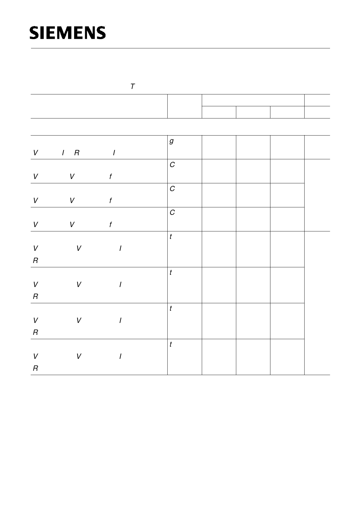
Electrical Characteristics, at Tj = 25°C, unless otherwise specified
Parameter
Symbol
Values
min.
typ.
max.
Dynamic Characteristics
Transconductance
VDSâ„ 2 * ID * RDS(on)max, ID = -0.37 A
Input capacitance
VGS = 0 V, VDS = 25 V, f = 1 MHz
Output capacitance
VGS = 0 V, VDS = 25 V, f = 1 MHz
Reverse transfer capacitance
VGS = 0 V, VDS = 25 V, f = 1 MHz
Turn-on delay time
VDD = -30 V, VGS = -10 V, ID = -0.29 A
RGS = 50 âŠ
Rise time
VDD = -30 V, VGS = -10 V, ID = -0.29 A
RGS = 50 âŠ
Turn-off delay time
VDD = -30 V, VGS = -10 V, ID = -0.29 A
RGS = 50 âŠ
Fall time
VDD = -30 V, VGS = -10 V, ID = -0.29 A
RGS = 50 âŠ
gfs
Ciss
Coss
Crss
td(on)
tr
td(off)
tf
0.25
-
-
-
-
-
-
-
0.35 -
270
360
50
75
15
25
8
12
30
45
80
110
90
120
Unit
S
pF
ns
Semiconductor Group
3
Sep-12-1996
Share Link: 