MAX5544CSA Ver la hoja de datos (PDF) - Maxim Integrated
Número de pieza
componentes Descripción
Fabricante
MAX5544CSA Datasheet PDF : 8 Pages
| |||
Low-Cost, +5V, Serial-Input,
Voltage-Output, 14-Bit DAC
Detailed Description
The MAX5544 voltage-output, 14-bit digital-to-analog
converter (DAC) offers 14-bit monotonicity with less
than 1LSB differential linearity error. Serial-data transfer
minimizes the number of package pins required.
The MAX5544 is composed of two matched DAC sec-
tions, with a 12-bit inverted R-2R DAC forming the
12LSBs and the 4MSBs derived from 15 identically
matched resistors. This architecture allows the lowest
glitch energy to be transferred to the DAC output on
major-carry transitions. It also decreases the DAC out-
put impedance by a factor of eight compared to a stan-
dard R-2R ladder, allowing unbuffered operation in
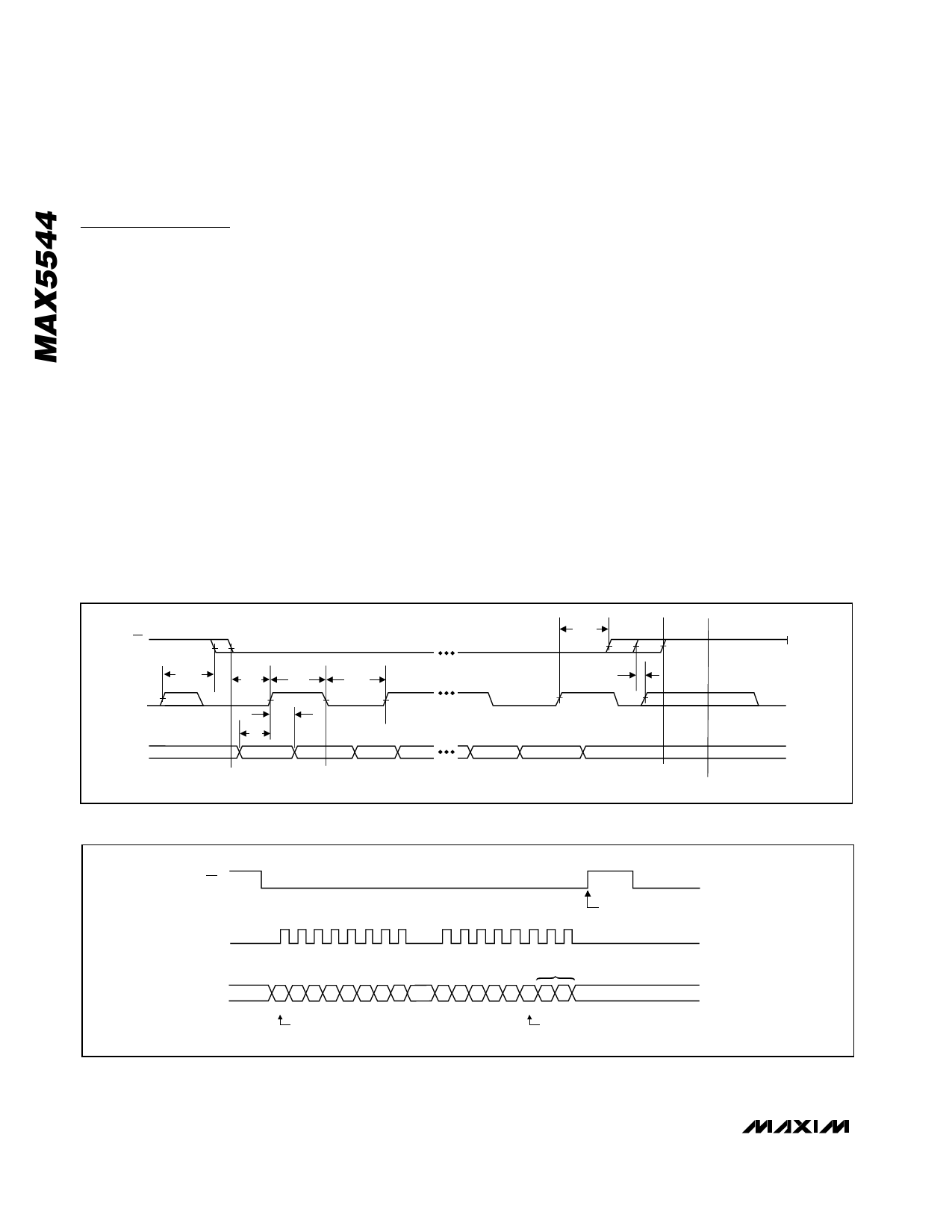
medium-load applications. Figure 1 is the timing dia-
gram.
Digital Interface
The MAX5544 digital interface is a standard 3-wire con-
nection compatible with SPI/QSPI/MICROWIRE inter-
faces. The chip-select input (CS) frames the serial data
loading at the data input pin (DIN). Immediately follow-
ing CS’s high-to-low transition, the data is shifted
synchronously and latched into the input register on the
rising edge of the serial-clock input (SCLK). After 16
data bits (14 data bits, plus two sub-bits set to zero)
have been loaded into the serial input register, it trans-
fers its contents to the DAC latch on CS’s low-to-high
transition (Figure 2). Note that if CS does not remain
low during the entire 16 SCLK cycles, data will be cor-
rupted. In this case, reload the DAC latch with a new
16-bit word.
External Reference
The MAX5544 operates with external voltage refer-
ences from 2V to 3V. The reference voltage determines
the DAC’s full-scale output voltage.
Power-On Reset
The MAX5544 has a power-on reset circuit to set the
DAC’s output to 0V in unipolar mode when VDD is first
applied. This ensures that unwanted DAC output volt-
ages will not occur immediately following a system
power-up, such as after power loss. In bipolar mode,
the DAC output is set to -VREF.
tCSH1
CS
;;;;;;;;; SCLK
tCSHO
DIN
tCSSO
tCH
tDH
tDS
D13
tCL
D12
tCSS1
S0
Figure 1. Timing Diagram
CS
; ; ;; SCLK
DIN
DAC
UPDATED
D13 D12 D11 D10 D9 D8 D7 D6
SUB-BITS
D5 D4 D3 D2 D1 D0 S1 S0
MSB
LSB
Figure 2. 3-Wire Interface Timing Diagram
6 _______________________________________________________________________________________
Share Link: 