MAX703 Ver la hoja de datos (PDF) - Maxim Integrated
Número de pieza
componentes Descripción
Fabricante
MAX703 Datasheet PDF : 10 Pages
| |||
MAX703/MAX704
Low-Cost Microprocessor Supervisory
Circuits with Battery Backup
Ensuring a Valid RESET Output
Down to VCC = 0V
When VCC falls below 1V, the MAX703/MAX704 RESET
output no longer sinks current; it becomes an open circuit.
High-impedance CMOS logic inputs can drift to unde-
termined voltages if left as open circuits. If a pulldown
resistor is added to the RESET pin as shown in Figure 6,
any stray charge or leakage currents will flow to ground,
holding RESET low. Resistor value R1 is not critical. It
should be about 100kΩ, which is large enough not to load
RESET and small enough to pull RESET to ground.
Replacing the Backup Battery
The backup battery can be removed while VCC remains
valid without triggering a reset. As long as VCC stays
above the reset threshold, battery-backup mode cannot
VCC
VOUT
MAX703
MAX704
VBATT
RESET
R1
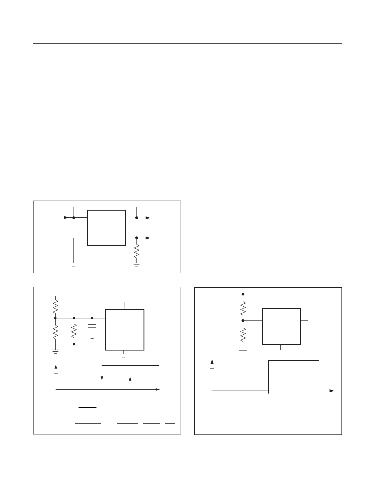
Figure 6. RESET Valid to Ground Circuit
VIN
R1
C1*
R2
R3
TOP
+5V
VCC
PFI
MAX703
MAX704
PFO GND
*OPTIONAL
be entered. This is an improvement on switchover ICs
that initiate a reset when VCC and VBATT are at or near
the same voltage level (regardless of the reset threshold
voltage). If the voltage on the unconnected VBATT pin
floats up toward VCC, this condition alone cannot initiate
a reset when using the MAX703/MAX704.
Adding Hysteresis to the
Power-Fail Comparator
Hysteresis adds a noise margin to the power-fail com-
parator and prevents repeated triggering of PFO when
VIN is near the power-fail comparator trip point. Figure 7
shows how to add hysteresis to the power-fail compara-
tor. Select the ratio of R1 and R2 so that PFI sees 1.25V
when VIN falls to the desired trip point (VTRIP). Resistor
R3 adds hysteresis. It will typically be an order of magni-
tude greater than R1 or R2. The current through R1 and
R2 should be at least 1μA to ensure that the 25nA (max)
PFI input current does not shift the trip point. R3 should
be larger than 10kΩ to prevent it from loading down the
PFO pin. Capacitor C1 adds additional noise rejection.
Monitoring a Negative Voltage
The power-fail comparator can be used to monitor a
negative supply voltage using Figure 8’s circuit. When
the negative supply is valid, PFO is low. When the nega-
tive supply voltage droops, PFO goes high. This circuit’s
accuracy is affected by the PFI threshold tolerance, the
VCC voltage, and resistors R1 and R2.
+5V
R1
R2
V-
VCC
PFI
PFO
MAX703
MAX704
GND
+5V
+5V
PFO
PFO
0V
0V
0V
VL VTRIP VH
VIN
VTRIP
=
1.25
R1 + R
R2
2
VTRIP
0V
V-
5 − 1.25 = 1.25 − VTRIP
VH
=
1.25
/
R 2||R 3
R1 + R 2||R
3
VL − 1.25 + 5 − 1.25 = 1.25
R1
R3
R2
R1
R2
NOTE: VTRIP IS NEGATIVE
Figure 7. Adding Hysteresis to the Power-Fail Comparator
Figure 8. Monitoring a Negative Voltage
www.maximintegrated.com
Maxim Integrated │ 7
Share Link: 