RF3140PCBA-41X Ver la hoja de datos (PDF) - RF Micro Devices
Número de pieza
componentes Descripción
Fabricante
RF3140PCBA-41X Datasheet PDF : 16 Pages
| |||
RF3140
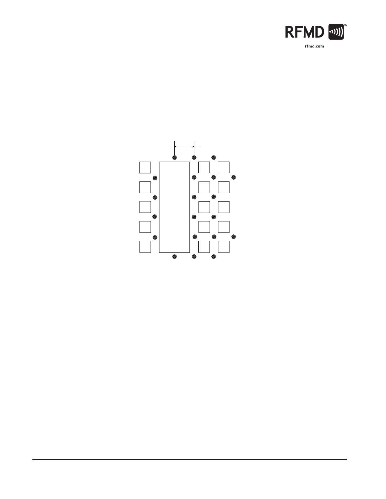
Thermal Pad and Via Design
The PCB land pattern has been designed with a thermal pad that matches the exposed die paddle size on the bottom of the
device.
Thermal vias are required in the PCB layout to effectively conduct heat away from the package. The via pattern shown has been
designed to address thermal, power dissipation and electrical requirements of the device as well as accommodating routing
strategies.
The via pattern used for the RFMD qualification is based on thru-hole vias with 0.203mm to 0.330mm finished hole size with
0.025mm plating on via walls. If micro vias are used in a design, it is suggested that the quantity of vias be increased by a 4:1
ratio to achieve similar results. .
1.40 (mm) Grid
Figure 2. Thermal Pad and Via Design (RFMD
16 of 16
7628 Thorndike Road, Greensboro, NC 27409-9421 · For sales or technical
support, contact RFMD at (+1) 336-678-5570 or sales-support@rfmd.com.
Rev A9 DS060217
Share Link: 