RF3140PCBA-41X Ver la hoja de datos (PDF) - RF Micro Devices
Número de pieza
componentes Descripción
Fabricante
RF3140PCBA-41X Datasheet PDF : 16 Pages
| |||
RF3140
PCB Design Requirements
PCB Surface Finish
The PCB surface finish used for RFMD’s qualification process is electroless nickel, immersion gold. Typical thickness is 3μinch
to 8μinch gold over 180μinch nickel.
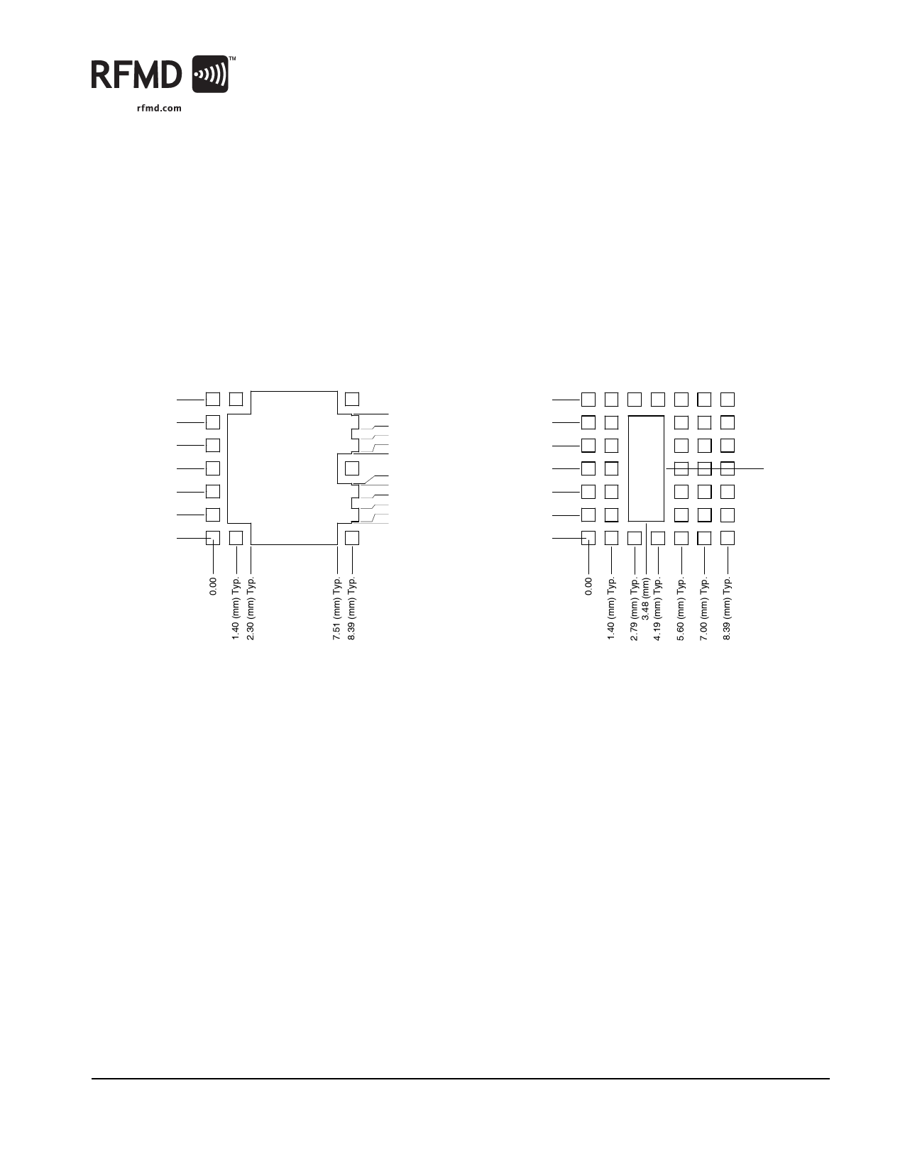
PCB Land Pattern Recommendation
PCB land patterns are based on IPC-SM-782 standards when possible. The pad pattern shown has been developed and tested
for optimized assembly at RFMD; however, it may require some modifications to address company specific assembly pro-
cesses. The PCB land pattern has been developed to accommodate lead and package tolerances.
PCB Metal Land and Solder Mask Pattern
A = 0.80 (mm) Sq. Typ.
Pin 1
8.39 (mm) Typ.
AA
7.00 (mm)
A
5.60 (mm)
A
4.20 (mm) Typ.
A
2.81 (mm)
A
1.40 (mm)
A
0.00
AA
A = 0.80 (mm) Sq. Typ.
B = 2.17 x 6.40 (mm)
Pin 1
A
8.39 (mm) Typ.
AAAAAAA
7.49 (mm) Typ.
6.60 (mm)
6.00 (mm)
5.20 (mm)
5.11 (mm)
7.00 (mm) Typ.
5.60 (mm) Typ.
AA
AA
AAA
AAA
A
3.30 (mm)
4.20 (mm) Typ.
AA
B
AAA
4.20 (mm)
3.21 (mm)
2.41 (mm)
2.81 (mm) Typ.
AA
AAA
1.78 (mm)
0.98 (mm)
0.89 (mm) Typ.
1.40 (mm) Typ.
AA
AAA
A
0.00
AAAAAAA
Metal Land Pattern
Figure 1. PCB Metal Land and Solder Mask Pattern (Top View)
Solder Mask Pattern
Rev A9 DS060217
7628 Thorndike Road, Greensboro, NC 27409-9421 · For sales or technical
support, contact RFMD at (+1) 336-678-5570 or sales-support@rfmd.com.
15 of 16
Share Link: 