RF2337 Ver la hoja de datos (PDF) - RF Micro Devices
Número de pieza
componentes Descripción
Fabricante
RF2337 Datasheet PDF : 4 Pages
| |||
RF2337
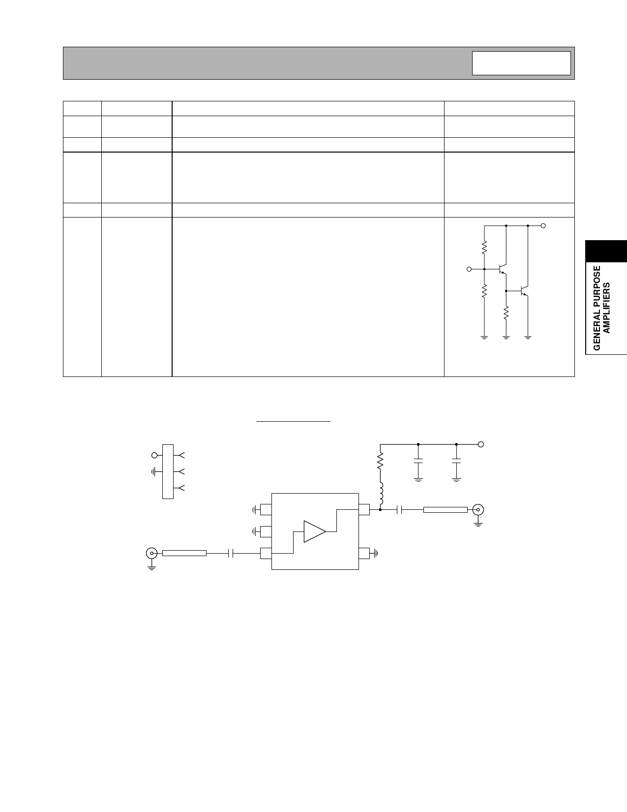
Pin Function Description
Interface Schematic
1
GND
Ground connection. Keep traces physically short and connect immedi-
ately to ground plane for best performance.
2
GND
Same as pin 1.
3
RF IN
RF input pin. This pin is NOT internally DC blocked. A DC blocking
capacitor, suitable for the frequency of operation, should be used in
most applications. DC coupling of the input is not allowed, because this
will override the internal feedback loop and cause temperature instabil-
ity.
4
GND
Same as pin 1.
5
RF OUT RF output and bias pin. Biasing is accomplished with an external series
resistor and choke inductor to VCC. The resistor is selected to set the
DC current into this pin to a desired level. The resistor value is deter-
mined by the following equation:
R = (---V----S--U----P---P----L---Y----–----V----D----E---V---I--C----E---)
RF IN
ICC
RF OUT
4
Care should also be taken in the resistor selection to ensure that the
current into the part never exceeds 75mA over the planned oper-
ating temperature. This means that a resistor between the supply and
this pin is always required, even if a supply near 3.6V is available, to
provide DC feedback to prevent thermal runaway. Because DC is
present on this pin, a DC blocking capacitor, suitable for the frequency
of operation, should be used in most applications. The supply side of
the bias network should also be well bypassed.
Evaluation Board Schematic
(Download Bill of Materials from www.rfmd.com.)
P1-1
P1
1 VCC
2 GND
3 NC
1
C1
2
J1
50 Ω µstrip
100 pF
RF IN
3
R1
22 Ω
C3
100 pF
C4
1 µF
VCC
P1-1
L1
100 nH
50 Ω µstrip
5
C2
100 pF
J2
RF OUT
4
233X410-
Rev A3 001201
4-157
Share Link: 