RF2365 Ver la hoja de datos (PDF) - RF Micro Devices
Número de pieza
componentes Descripción
Fabricante
RF2365 Datasheet PDF : 8 Pages
| |||
RF2365
Pin Function Description
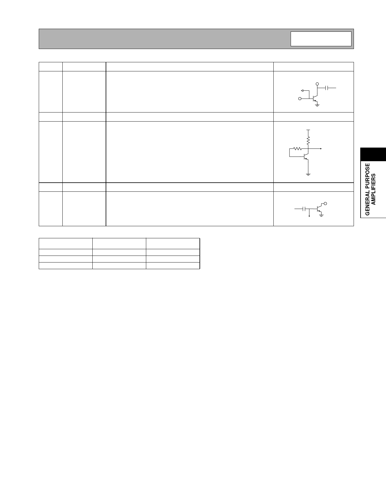
1
RF IN
RF input pin. This pin is DC coupled.
Interface Schematic
PD
To Bias
Circuit
RF IN
2
GND1
Ground connection. See evaluation board schematic notes.
3
PD
Power down pin. This pin serves as the interstage for the 2-stage LNA.
An inductor is required to pull pin 3 to VCC (see application schematic).
If desired, this voltage can be lowered to trade off IP3 versus ICC,TOTAL.
(See table below.)
GND1
PD
To RF
Stages
4
4
GND2
Ground connection. See evaluation board schematic notes.
5
RF OUT Amplifier Output pin. This pin is an open-collector output. It must be
biased to either VCC or pin 4 through a choke or matching inductor.
This pin is typically matched to 50Ω with a shunt bias/matching induc-
tor and series blocking/matching capacitor. Refer to application sche-
matics.
R1
0Ω
75 Ω
150 Ω
IIP3
+4.0 dBm
+2.0 dBm
-3.5 dBm
ICC
8.0 mA
6.5 mA
5.0 mA
To Bias GND2
Circuit
Rev A4 001201
4-217
Share Link: 