RF2326PCBA Ver la hoja de datos (PDF) - RF Micro Devices
Número de pieza
componentes Descripción
Fabricante
RF2326PCBA Datasheet PDF : 8 Pages
| |||
Preliminary
RF2326
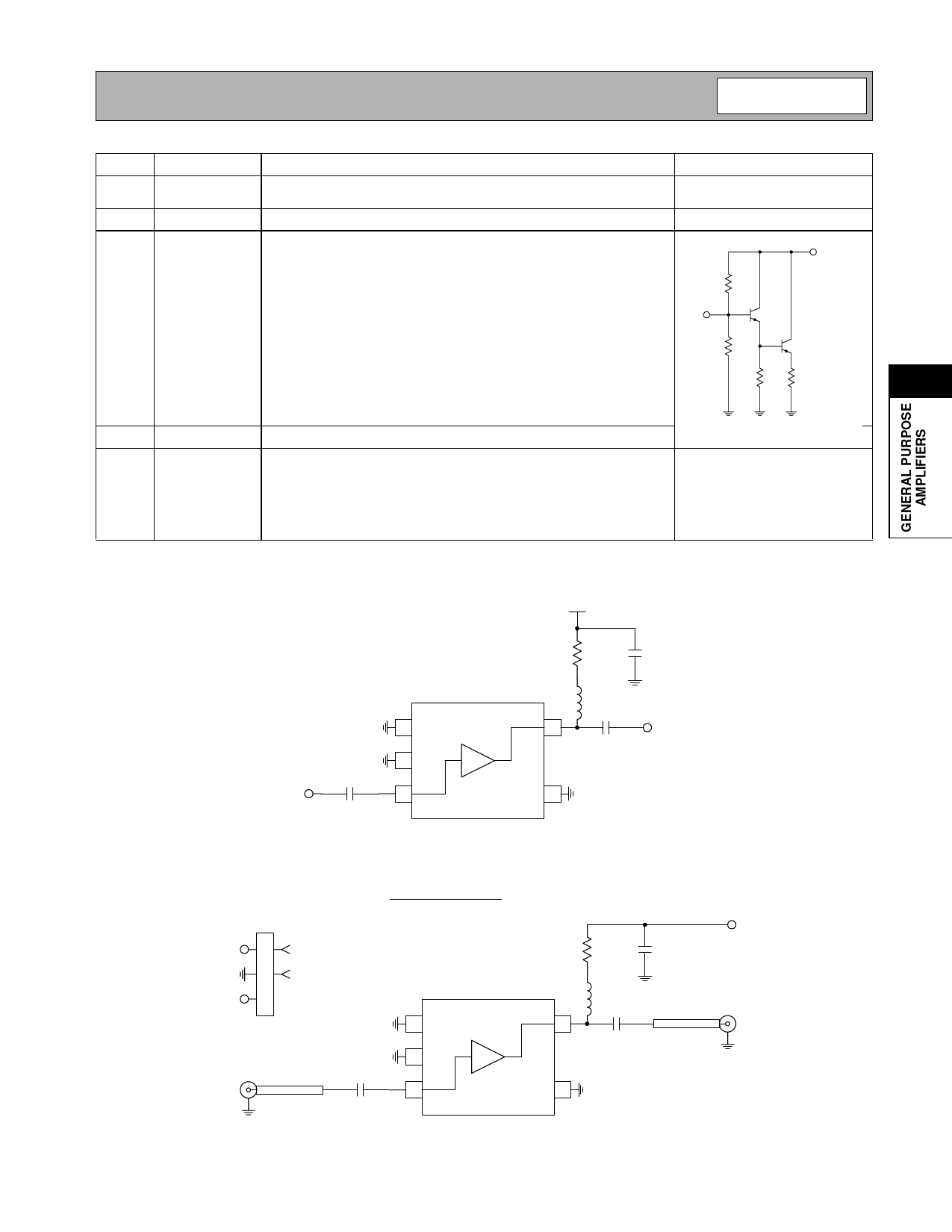
Pin Function Description
Interface Schematic
1
GND
Ground connection. Keep traces physically short and connect immedi-
ately to ground plane for best performance.
2
GND
Same as pin 1.
3
RF IN
RF input pin. This pin is not externally DC blocked and thus requires an
external blocking capacitor suitable for the frequency of operation. The
input impedance of this pin is internally matched to 50Ω using resistive
feedback.
RF OUT
RF IN
4
4
GND
Same as pin 1.
5
RF OUT RF output and bias pin. The input impedance of this pin is internally See pin 3 schematic.
matched to 50Ω using resistive feedback. Bias should be supplied to
this pin through an external series resistor and RF choke inductor.
Because DC biasing is present on this pin, a DC blocking capacitor
should be used in most applications (see application schematic). The
supply side of the bias network should be well-bypassed.
Application Schematic
VCC
36 Ω
1 nF
1
2
100 pF
RF IN
3
120 nH
5
100 pF
RF OUT
4
Evaluation Board Schematic
(Download Bill of Materials from www.rfmd.com.)
P1
P1-1 1 VCC
2 GND
NC
3
1
C1
2
RF IN
50 Ω µstrip
100 pF
J1
3
R1
36 Ω
C5
1 nF
L2
120 nH
50 Ω µstrip
5
C2
100 pF
4
P1-1
RF OUT
J2
Rev A4 010720
4-131
Share Link: 