CAT25C32LA-TE13 Ver la hoja de datos (PDF) - Catalyst Semiconductor => Onsemi
Número de pieza
componentes Descripción
Fabricante
CAT25C32LA-TE13 Datasheet PDF : 11 Pages
| |||
CAT25C32/64
Byte Write
Once the device is in a Write Enable state, the user
may proceed with a write sequence by setting the CS
low, issuing a write instruction via the SI line, followed
by the 16-bit address (the three Most Significant Bits
are don’t care for 25C64 and four most significant bits
are don't care for 25C32), and then the data to be
written. Programming will start after the CS is brought
high. Figure 6 illustrates byte write sequence.
During an internal write cycle, all commands will be
ignored except the RDSR (Read Status Register)
instruction.
The Status Register can be read to determine if the
write cycle is still in progress. If Bit 0 of the Status
Register is set at 1, write cycle is in progress. If Bit 0
is set at 0, the device is ready for the next instruction.
Page Write
The CAT25C32/64 features page write capability.
After the first initial byte the host may continue to write
up to 64 bytes of data to the CAT25C32/64. After each
byte of data is received, six lower order address bits
are internally incremented by one; the high order bits of
address will remain constant. The only restriction is that the
64 bytes must reside on the same page. If the address
counter reaches the end of the page and clock continues,
the counter will “roll over” to the first address of the page
and overwrite any data that may have been written. The
CAT25C32/64 is automatically returned to the write disable
state at the completion of the write cycle. Figure 8 illustrates
the page write sequence.
To write to the status register, the WRSR instruction should
be sent. Only Bit 2, Bit 3 and Bit 7 of the status register can
be written using the WRSR instruction. Figure 7 illustrates
the sequence of writing to status register.
DESIGN CONSIDERATIONS
The CAT25C32/64 powers up in a write disable state and
in a low power standby mode. A WREN instruction must be
issued to perform any writes to the device after power up.
Also,on power up CS should be brought low to enter a ready
state and receive an instruction. After a successful byte/
page write or status register write the CAT25C32/64 goes
into a write disable mode. CS must be set high after the
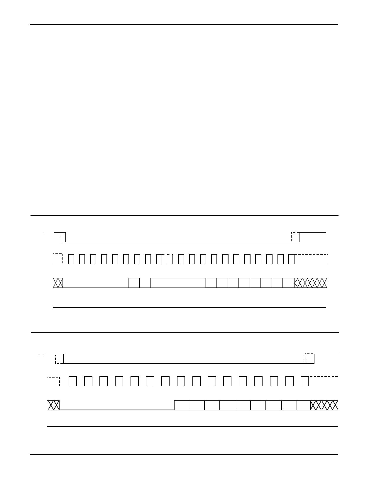
Figure 6. Write Instruction Timing
CS
012345678
21 22 23 24 25 26 27 28 29 30 31
SK
OPCODE
SI
00 00 00 10
ADDRESS
DATA IN
D7 D6 D5 D4 D3 D2 D1 D0
SO
HIGH IMPEDANCE
Note: Dashed Line= mode (1, 1) – – – –
Figure 7. WRSR Instruction Timing
CS
SCK
0
1
2
3
4
5
6
7
8
9 10 11 12 13 14 15
OPCODE
DATA IN
SI
0
0
0
0
00
0
1
7
6
5
4
32
10
MSB
SO
HIGH IMPEDANCE
Note: Dashed Line= mode (1, 1) — — — —
Doc. No. 1001, Rev. G
8
Share Link: 