CAT25C32L-TE13 Ver la hoja de datos (PDF) - Catalyst Semiconductor => Onsemi
Número de pieza
componentes Descripción
Fabricante
CAT25C32L-TE13 Datasheet PDF : 11 Pages
| |||
CAT25C32/64
the communication between the microcontroller and the
25C32/64. Opcodes, byte addresses, or data present on
the SI pin are latched on the rising edge of the SCK. Data
on the SO pin is updated on the falling edge of the SCK.
CS: Chip Select
CS is the Chip select pin. CS low enables the CAT25C32/
64 and CS high disables the CAT25C32/64. CS high
takes the SO output pin to high impedance and forces
the devices into a Standby Mode (unless an internal
write operation is underway). The CAT25C32/64 draws
ZERO current in the Standby mode. A high to low
transition on CS is required prior to any sequence being
initiated. A low to high transition on CS after a valid write
sequence is what initiates an internal write cycle.
WP: Write Protect
WP is the Write Protect pin. The Write Protect pin will
allow normal read/write operations when held high.
When WP is tied low and the WPEN bit in the status
register is set to “1”, all write operations to the status
register are inhibited. WP going low while CS is still low
will interrupt a write to the status register. If the internal
write cycle has already been initiated, WP going low will
have no effect on any write operation to the status
register. The WP pin function is blocked when the WPEN
bit is set to 0.
HOLD: Hold
The HOLD pin is used to pause transmission to the
CAT25C32/64 while in the middle of a serial sequence
without having to re-transmit entire sequence at a later
time. To pause, HOLD must be brought low while SCK
is low. The SO pin is in a high impedance state during the
time the part is paused, and transitions on the SI pins will
be ignored. To resume communication, HOLD is brought
high, while SCK is low. (HOLD should be held high any
time this function is not being used.) HOLD may be tied
high directly to Vcc or tied to Vcc through a resistor.
Figure 9 illustrates hold timing sequence.
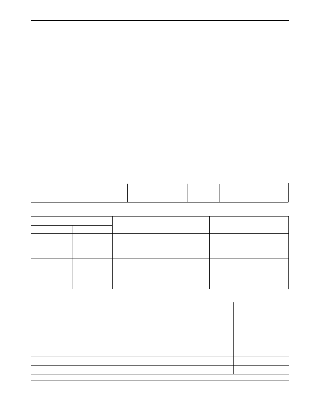
STATUS REGISTER
7
6
5
WPEN
X
X
BLOCK PROTECTION BITS
Status Register Bits
BP1
BP0
0
0
0
1
1
0
1
1
WRITE PROTECT ENABLE OPERATION
WPEN
0
0
1
1
X
X
WP
X
X
Low
Low
High
High
WEL
0
1
0
1
0
1
4
3
2
1
0
X
BP1
BP0
WEL
RDY
Array Address
Protected
None
25C32: 0C00-0FFF
25C64:1800-1FFF
25C32: 800-0FFF
25C64:1000-1FFF
25C32: 0000-0FFF
25C64:0000-1FFF
Protection
No Protection
Quarter Array Protection
Half Array Protection
Full Array Protection
Protected
Blocks
Protected
Protected
Protected
Protected
Protected
Protected
Unprotected
Blocks
Protected
Writable
Protected
Writable
Protected
Writable
Status
Register
Protected
Writable
Protected
Protected
Protected
Writable
5
Doc. No. 1001, Rev. G
Share Link: 