MCM32515 Ver la hoja de datos (PDF) - Motorola => Freescale
Número de pieza
componentes Descripción
Fabricante
MCM32515 Datasheet PDF : 8 Pages
| |||
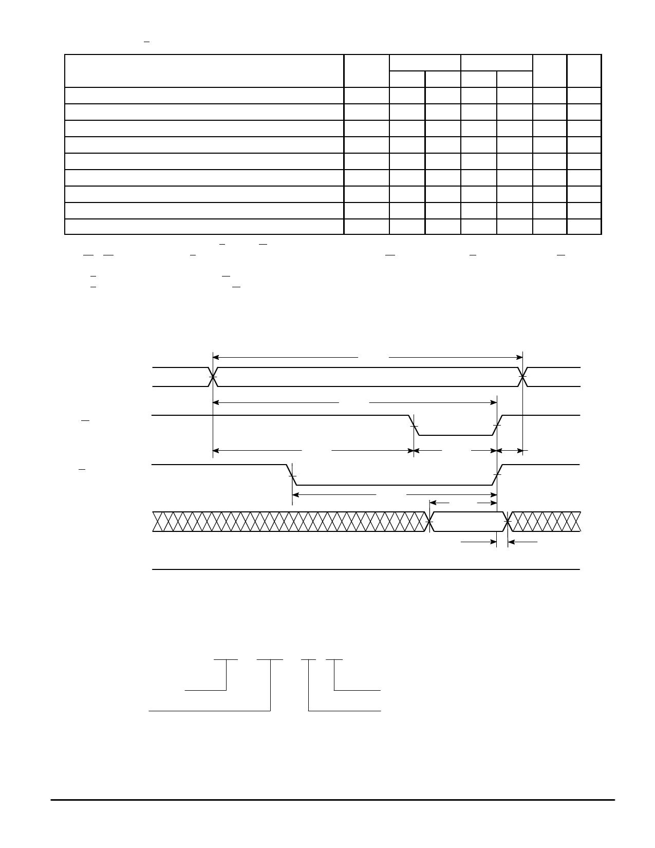
WRITE CYCLE 2 (E Controlled, See Notes 1 and 2)
MCM32515–20 MCM32515–25
Parameter
Symbol Min Max Min Max Unit Notes
Write Cycle Time
tAVAV
20
—
25
—
ns
3
Address Setup Time
tAVEL
0
—
0
—
ns
Address Valid to End of Write
tAVEH
15
—
17
—
ns
Enable to End of Write
tELEH
15
—
17
—
ns
4,5
Enable to End of Write
tELWH
15
—
17
—
ns
Write Pulse Width
tWLEH
15
—
17
—
ns
Data Valid to End of Write
tDVEH
10
—
10
—
ns
Data Hold Time
tEHDX
0
—
0
—
ns
Write Recovery Time
tEHAX
0
—
0
—
ns
NOTES:
1. A write occurs during the overlap of E low and W low.
2. E1 – E4 are represented by E in these timing specifications, any combination of Exs may be asserted. G is a don’t care when W is low.
3. All write cycle timing is referenced from the last valid address to the first transitioning address.
4. If E goes low coincident with or after W goes low, the output will remain in a high impedance condition.
5. If E goes high coincident with or before W goes high, the output will remain in a high impedance condition.
A (ADDRESS)
Ex (BYTE ENABLE)
W (WRITE ENABLE)
D (DATA IN)
Q (DATA OUT)
WRITE CYCLE 2
tAVAV
tAVEH
tAVEL
tWLEH
HIGH–Z
tELEH
tELWH
tDVEH
DATA VALID
tEHAX
tEHDX
Motorola Memory Prefix
Part Number
ORDERING INFORMATION
(Order by Full Part Number)
MCM 32515 XX XX
Speed (20 = 20 ns, 25 = 25 ns)
Package (SG = Gold Pad SIMM)
Full Part Numbers — MCM32515SG20 MCM32515SG25
MOTOROLA FAST SRAM
MCM32515
7
Share Link: 