HV9910BLG-G(2007) Ver la hoja de datos (PDF) - Supertex Inc
Número de pieza
componentes Descripción
Fabricante
HV9910BLG-G Datasheet PDF : 8 Pages
| |||
HV9910B
Pin Description
Function
VIN
Description
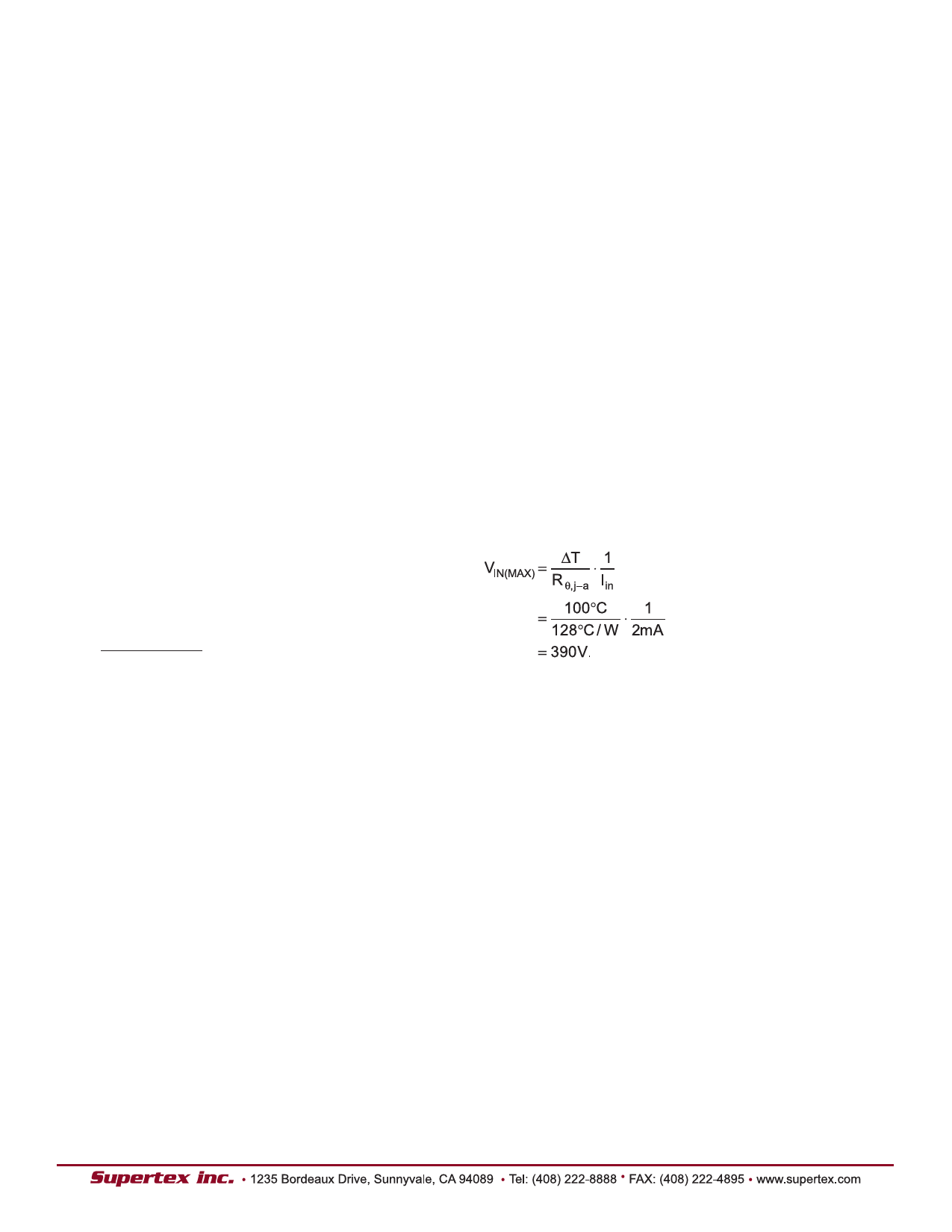
This pin is the input of an 8V – 450V linear regulator.
VDD
This is the power supply pin for all internal circuits.
It must be bypassed with a low ESR capacitor to GND (≥ 0.1μF).
GATE
This pin is the output gate driver for an external N-channel power MOSFET.
GND
Ground return for all internal circuitry. This pin must be electrically connected to the ground of the power
train.
PWMD
This is the PWM dimming input of the IC. When this pin is pulled to GND, the gate driver is turned off.
When the pin is pulled high, the gate driver operates normally.
This pin is the current sense pin used to sense the FET current by means of an external sense resistor.
CS
When this pin exceeds the lower of either the internal 250mV or the voltage at the LD pin, the gate output
goes low.
LD
This pin is the linear dimming input and sets the current sense threshold as long as the voltage at the pin
is less than 250mV (typ).
This pin sets the oscillator frequency. When a resistor is connected between RT and GND, the HV9910B
RT
operates in constant frequency mode. When the resistor is connected between RT and GATE, the IC
operates in constant off-time mode.
NC
No connection
Block Diagram
VIN
Regulator
LD
-
+
CS
+
250mV -
POR
Blanking
RQ
S
Oscillator
GND
RT
PWMD
VDD
GATE
4
Share Link: 