HV9910BLG-G(2007) Ver la hoja de datos (PDF) - Supertex Inc
Número de pieza
componentes Descripción
Fabricante
HV9910BLG-G Datasheet PDF : 8 Pages
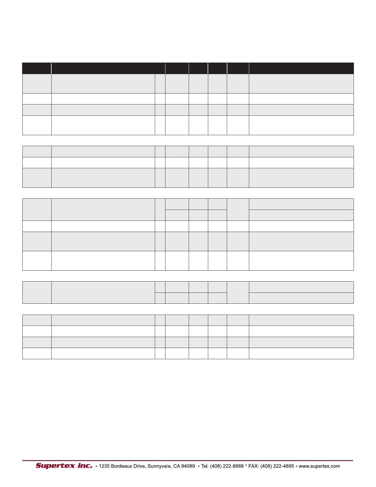
| |||
HV9910B
Internal Regulator (cont.)
Symbol Description
Min Typ Max Units Conditions
ΔVDD, load Load Regulation of VDD
-0
-
100 mV IDD(ext) = 0 – 1mA, 500pF at GATE;
RT = 226kΩ, PWMD = VDD
UVLO VDD undervoltage lockout threshold * 6.45 6.7 6.95 V VIN rising
∆UVLO VDD undervoltage lockout hysteresis #
-
500 -
mV VIN falling
IIN,MAX
Current that the regulator can
supply before IC goes into UVLO
#
5
-
-
mA VIN = 8V
PWM Dimming
VEN(lo)
VEN(hi)
Pin PWMD input low voltage
Pin PWMD input high voltage
REN
Pin PWMD pull-down resistance
at PWMD
*-
* 2.4
-
1.0
V VIN = 8V – 450V
-
-
V VIN = 8V – 450V
- 50 100 150 kΩ VPWMD = 5.0V
Current Sense Comparator
VCS,TH
VOFFSET
T
BLANK
Current sense pull-in threshold
voltage
Offset voltage for LD comparator
Current sense blanking interval
- 225 250 275 mV -40°C < TA < +85°C
213 250 287
TA < +125°C
* -12
- 12 mV ---
* 150 215 280 ns ---
tDELAY
Delay to output
-
-
80 150
ns
VLD = VDD,
VCS = VCS,TH + 50mV after TBLANK
Oscillator
fOSC
Oscillator frequency
GATE Driver
- 20 25 30
R = 1.00MΩ
kHz
T
- 80 100 120
RT = 226kΩ
ISOURCE Gate sourcing current
- 0.165 -
-
A
VGATE = 0V
I
Gate sinking current
SINK
- 0.165 -
-
A V =V
GATE
DD
tRISE
GATE output rise time
-
-
30 50
ns CGATE = 500pF
tFALL
GATE output fall time
-
-
30 50
ns CGATE = 500pF
(1) Also limited by package power dissipation limit, whichever is lower.
(†) VDD load current external to the HV9910B
* Specifications that apply over the full temperature range are guaranteed by design and characterization
# Guaranteed by design
3
Share Link: 