HV9910B(2007) Ver la hoja de datos (PDF) - Supertex Inc
Número de pieza
componentes Descripción
Fabricante
HV9910B Datasheet PDF : 8 Pages
| |||
HV9910B
Ordering Information
Device
Package Options
8-Lead SO
16-Lead SO
HV9910B
HV9910BLG-G HV9910BNG-G
-G indicates package is RoHS compliant (‘Green’)
Absolute Maximum Ratings
Parameter
Value
VIN to GND
CS, LD, PWMD, GATE, RT
VDD to GND
Junction Temperature Range
-0.5V to +470V
-0.3V to (V + 0.3V)
DD
12V
-40°C to +150°C
Storage Temperature Range
-65°C to +150°C
Continuous Power Dissipation
(TA = +25°C)
8-Lead SO
16-Lead SO
830mW
1300mW
Stresses beyond those listed under “Absolute Maximum Ratings” may
cause permanent damage to the device. These are stress ratings only,
and functional operation of the device at these or any other conditions
beyond those indicated in the operational sections of the specifications is
not implied. Exposure to absolute maximum rating conditions for extended
periods may affect device reliability.
Thermal Impedence
8-Lead SO (LG)
16-Lead SO (NG)
128OC/W
82OC/W
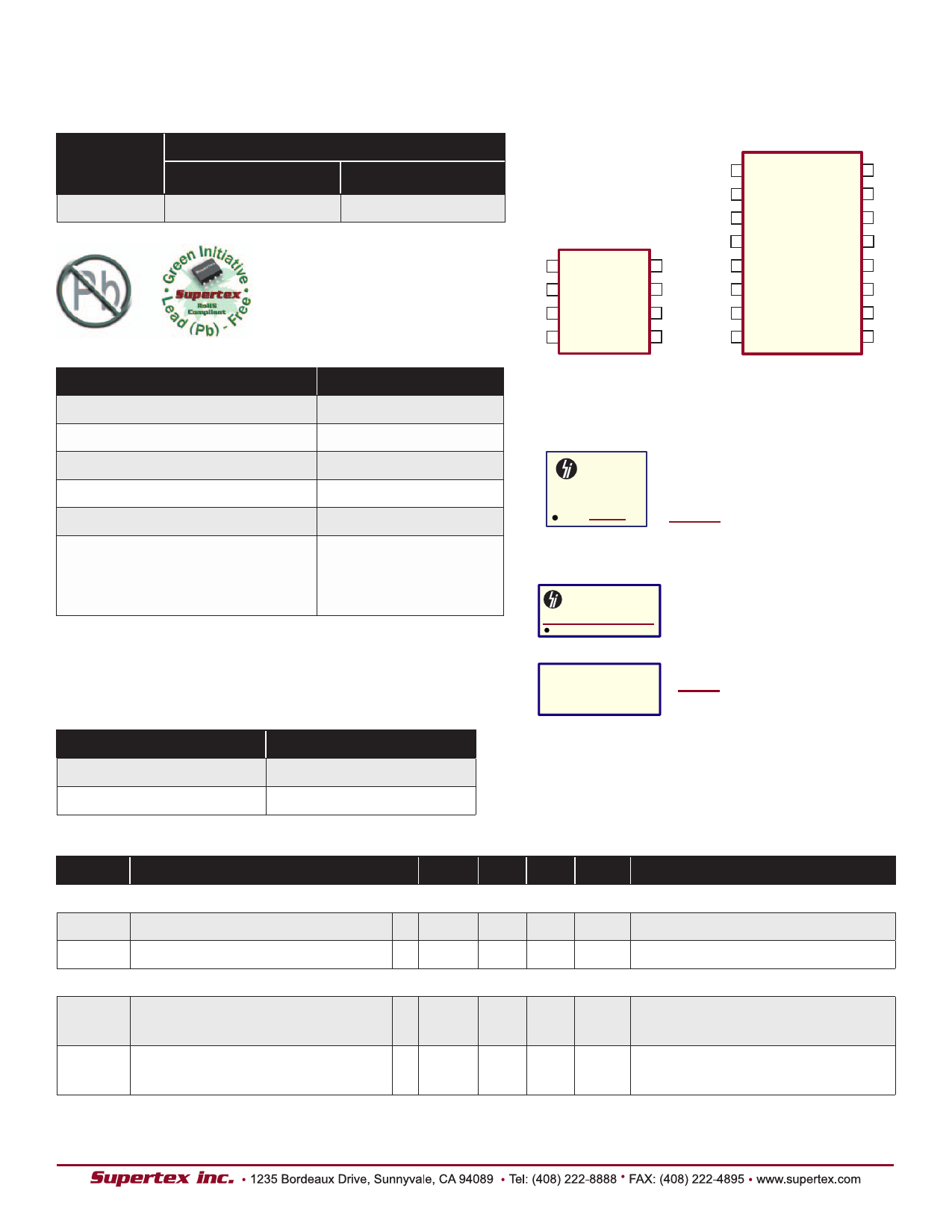
Pin Description
1 VIN
RT 8
2 CS
LD 7
3 GND
VDD 6
4 GATE PWMD 5
8-Lead SO (LG)
1 VIN
2 NC
3 NC
4 CS
5 GND
6 NC
7 NC
8 GATE
NC 16
NC 15
RT 14
LD 13
VDD 12
NC 11
NC 10
PWMD 9
16-Lead SO (NG)
Product Marking
YWW
9910B
LLLL
Y = Last Digit of Year Sealed
WW = Week Sealed
L = Lot Number
= “Green” Packaging
8-Lead SO (LG)
Top Marking
HV9910BNG
YWW LLLLLLLL
Bottom Marking
CCCCCCCCC AAA
Y = Last Digit of Year Sealed
WW = Week Sealed
L = Lot Number
C = Country of Origin*
A = Assembler ID*
= “Green” Packaging
*May be part of top marking
16-Lead SO (NG)
Electrical Characteristics (The * denotes specifications which apply over the full operating ambient temperature range of -40°C<TA<125°C.
Otherwise specifications are at TA= 25°C. VIN = 12V, unless otherwise noted. All Typical Numbers are at TA = 25°C )
Symbol Description
Min Typ Max Units Conditions
Input
VINDC
Input DC supply voltage range(1)
IINSD
Shut-Down mode supply current
Internal Regulator
* 8.0
- 450 V DC input voltage
-
-
0.5 1 mA Pin PWMD to GND
VDD
Internally regulated voltage
ΔVDD, line Line Regulation of VDD
- 7.25 7.5 7.75
V
VIN
=
8V,
I (†)
DD(ext)
=
0,
500pF
at
GATE; RT = 226kΩ, PWMD = VDD
-0
VIN = 8 - 450V, IDD(ext) = 0,
-
1
V 500pF at GATE; RT = 226kΩ,
PWMD = VDD
2
Share Link: 