HI5805 Ver la hoja de datos (PDF) - Renesas Electronics
Número de pieza
componentes Descripción
Fabricante
HI5805 Datasheet PDF : 12 Pages
| |||
HI5805
Absolute Maximum Ratings
Supply Voltage, AVCC or DVCC to AGND or DGND. . . . . . . . . +6.0V
DGND to AGND. . . . . . . . . . . . . . . . . . . . . . . . . . . . . . . . . . . . . . 0.3V
Digital I/O Pins . . . . . . . . . . . . . . . . . . . . . . . . . . . . . .DGND to DVCC
Analog I/O Pins . . . . . . . . . . . . . . . . . . . . . . . . . . . . . AGND to AVCC
Operating Conditions
Temperature Range, HI5805BIB . . . . . . . . . . . . . . . . -40oC to 85oC
Thermal Information
Thermal Resistance (Typical, Note 1)
JA (oC/W)
SOIC Package . . . . . . . . . . . . . . . . . . . . . . . . . . . . .
70
Maximum Junction Temperature . . . . . . . . . . . . . . . . . . . . . . .150oC
Maximum Storage Temperature Range . . . . . . . . . -65oC to 150oC
Maximum Lead Temperature (Soldering, 10s) . . . . . . . . . . . .300oC
(SOIC - Lead Tips Only)
CAUTION: Stresses above those listed in “Absolute Maximum Ratings” may cause permanent damage to the device. This is a stress only rating and operation of the
device at these or any other conditions above those indicated in the operational sections of this specification is not implied.
NOTE:
1. JA is measured with the component mounted on an evaluation PC board in free air.
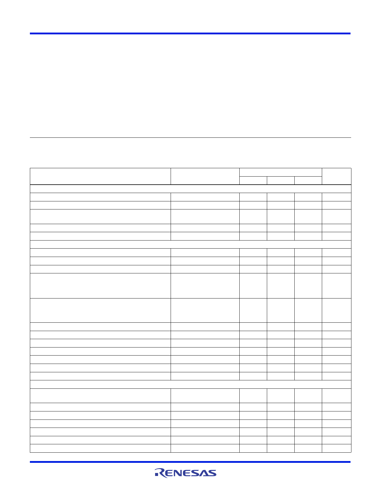
Electrical Specifications
TAAVC=C-4=0DoCVCtoC815=oCD,VDCiCff2er=enDtiVaCl ACn3a=lo+g5I.n0pVu,tf,ST=yp5icMaSl VPaSluaets5a0r%e
Duty
Test
RCeysculelt,sVaRtI2N5=oC3.,5V,
CL
=
10pF,
Unless Otherwise Specified
HI5805BIB (-40oC TO 85oC)
PARAMETER
TEST CONDITION
MIN
TYP
MAX
UNITS
ACCURACY
Resolution
12
-
-
Bits
Integral Linearity Error, INL
Differential Linearity Error, DNL
(Guaranteed No Missing Codes)
fIN = DC
fIN = DC
-
1
2
LSB
-
0.5
1
LSB
Offset Error, VOS
Full Scale Error, FSE
DYNAMIC CHARACTERISTICS
fIN = DC
fIN = DC
-
19
-
LSB
-
32
-
LSB
Minimum Conversion Rate
No Missing Codes
-
0.5
-
MSPS
Maximum Conversion Rate
No Missing Codes
5
-
-
MSPS
Effective Number of Bits, ENOB
Signal to Noise and Distortion Ratio, SINAD
=
----------------R----M-----S------S----i-g----n---a---l---------------
RMS Noise + Distortion
fIN = 1MHz
fIN = 1MHz
10.0
11
-
Bits
-
68
-
dB
Signal to Noise Ratio, SNR
=
R-----M-----S------S----i-g---n----a---l
RMS Noise
fIN = 1MHz
-
68
-
dB
Total Harmonic Distortion, THD
2nd Harmonic Distortion
3rd Harmonic Distortion
Spurious Free Dynamic Range, SFDR
Intermodulation Distortion, IMD
Transient Response
Over-Voltage Recovery
ANALOG INPUT
Maximum Peak-to-Peak Differential Analog Input Range
(VIN+ - VIN-)
Maximum Peak-to-Peak Single-Ended Analog Input Range
Analog Input Resistance, RIN
Analog Input Capacitance, CIN
Analog Input Bias Current, IB+ or IB-
Differential Analog Input Bias Current IB DIFF = (IB+ - IB-)
Full Power Input Bandwidth, FPBW
fIN = 1MHz
fIN = 1MHz
fIN = 1MHz
fIN = 1MHz
f1 = 1MHz, f2 = 1.02MHz
0.2V Overdrive
(Notes 2, 3)
(Note 3)
-
-80
-
dBc
-
-86
dBc
-
-83
-
dBc
-
83
-
dBc
-
-68
-
dBc
-
1
-
Cycle
-
2
-
Cycle
-
2.0
-
V
-
4.0
-
V
1
-
-
M
-
10
-
pF
-10
-
+10
A
-
0.5
-
A
-
100
-
MHz
FN3984 Rev 7.00
March 31, 2005
Page 3 of 12
Share Link: 