HI7190 Ver la hoja de datos (PDF) - Renesas Electronics
Número de pieza
componentes Descripción
Fabricante
HI7190 Datasheet PDF : 25 Pages
| |||
HI7190
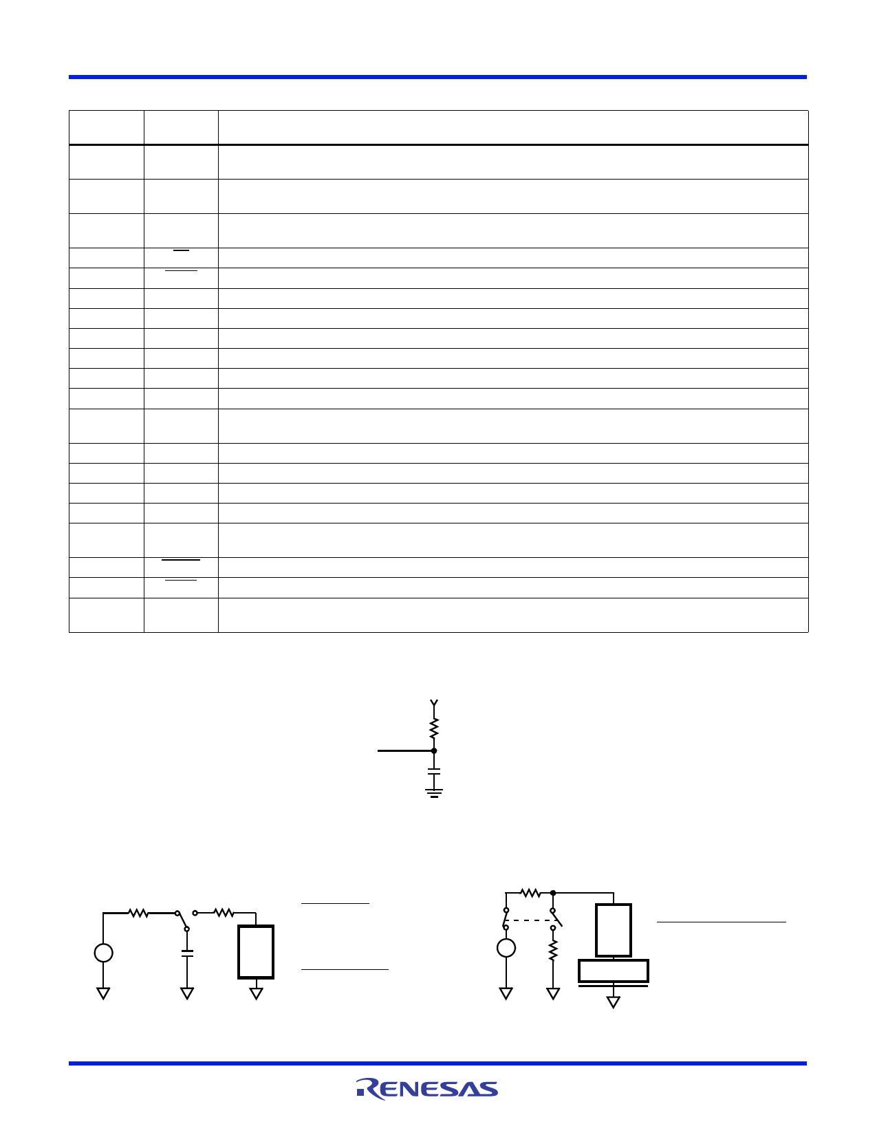
Pin Descriptions
20 LEAD
DIP, SOIC
1
2
3
4
5
6
7
8
9
10
11
12
13
14
15
16
17
18
19
20
PIN NAME
SCLK
SDO
SDIO
CS
DRDY
DGND
AVSS
VRLO
VRHI
VCM
VINLO
VINHI
AVDD
AGND
DVDD
OSC2
OSC1
RESET
SYNC
MODE
DESCRIPTION
Serial Interface Clock. Synchronizes serial data transfers. Data is input on the rising edge and output on the
falling edge.
Serial Data OUT. Serial data is read from this line when using a 3-wire serial protocol such as the
Motorola Serial Peripheral Interface.
Serial Data IN or OUT. This line is bidirectional programmable and interfaces directly to the Intel Standard Serial
Interface using a 2-wire serial protocol.
Chip Select Input. Used to select the HI7190 for a serial data transfer cycle. This line can be tied to DGND.
An Active Low Interrupt indicating that a new data word is available for reading.
Digital Supply Ground.
Negative Analog Power Supply (-5V).
External Reference Input. Should be negative referenced to VRHI.
External Reference Input. Should be positive referenced to VRLO.
Common Mode Input. Should be set to halfway between AVDD and AVSS.
Analog Input LO. Negative input of the PGIA.
Analog Input HI. Positive input of the PGIA. The VINHI input is connected to a current source that can be used to check
the condition of an external transducer. This current source is controlled via the Control Register.
Positive Analog Power Supply (+5V).
Analog Supply Ground.
Positive Digital Supply (+5V).
Used to connect a crystal source between OSC1 and OSC2. Leave open otherwise.
Oscillator Clock Input for the device. A crystal connected between OSC1 and OSC2 will provide a clock to the device,
or an external oscillator can drive OSC1. The oscillator frequency should be 10MHz (Typ).
Active Low Reset Pin. Used to initialize the HI7190 registers, filter and state machines.
Active Low Sync Input. Used to control the synchronization of a number of HI7190s. A logic ‘0’ initializes the converter.
Mode Pin. Used to select between Synchronous Self Clocking (Mode = 1) or Synchronous External Clocking
(Mode = 0) for the Serial Port.
Load Test Circuit
V1
DUT
R1
CL (INCLUDES STRAY
CAPACITANCE)
FIGURE 4.
ESD Test Circuits
R1
R2
V
CESD DUT
FIGURE 5A.
HUMAN BODY
CESD = 100pF
R1 = 10M
R2 = 1.5k
MACHINE MODEL
CESD = 200pF
R1 = 10M
R2 = 0
R1
V
R2
DUT
CHARGED DEVICE MODEL
R1 = 1G
R2 = 1
DIELECTRIC
FIGURE 5B.
FN3612 Rev 10.00
June 27, 2006
Page 7 of 25
Share Link: 