MSM6665-XX Ver la hoja de datos (PDF) - Oki Electric Industry
Número de pieza
componentes Descripción
Fabricante
MSM6665-XX
Oki Electric Industry

MSM6665-XX Datasheet PDF : 30 Pages
| |||
¡ Semiconductor
MSM6665-xx
If 1/9 duty is selected, common outputs C10 to C17 should be set open.
• TEST1, TEST2, TEST3
Test signal input pins.
The manufacturer uses these pins for testing.
The user should connect this pin to GND or leave open.
• OSC1, OSC2, OSC3
Pins used for 80kHz RC oscillation circuit formation and as external master clock input
pin. Leave OSC2 and OSC3 open during input of external master clock.
OSC1
OSC2
OSC3
10k W
76±5k W
56pF
OSC1
OSC2
OPEN
OSC3
OPEN
80kHz
[RC oscillation circuit formation]
[External master clock input]
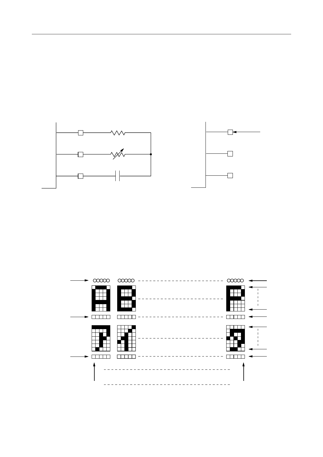
< Oscillation circuit wiring diagram >
• C1 - C17, S1 - S80 (Common 1 - 17, Segment 1 - 80)
LCD output pins to be connected with the LCD panel. Turning into AC is made by frame
inversion.
Use the C1 to C9 pins during use at 1/9 duty, and leave the C10 to C17 pins open.
ÆRefer to "Relationship between panel and LCD output".
Arbitrator
C1
C2
C8
Cursor
C9
C10
C16
Cursor
C17
S1
S80
<Relationship between panel and LCD output>
• VDD, VSS
Supply voltage pins. VDD should be set at "H" level.
9/30
Share Link: