RT9164A-15 Ver la hoja de datos (PDF) - Richtek Technology
Número de pieza
componentes Descripción
Fabricante
RT9164A-15 Datasheet PDF : 13 Pages
| |||
Preliminary
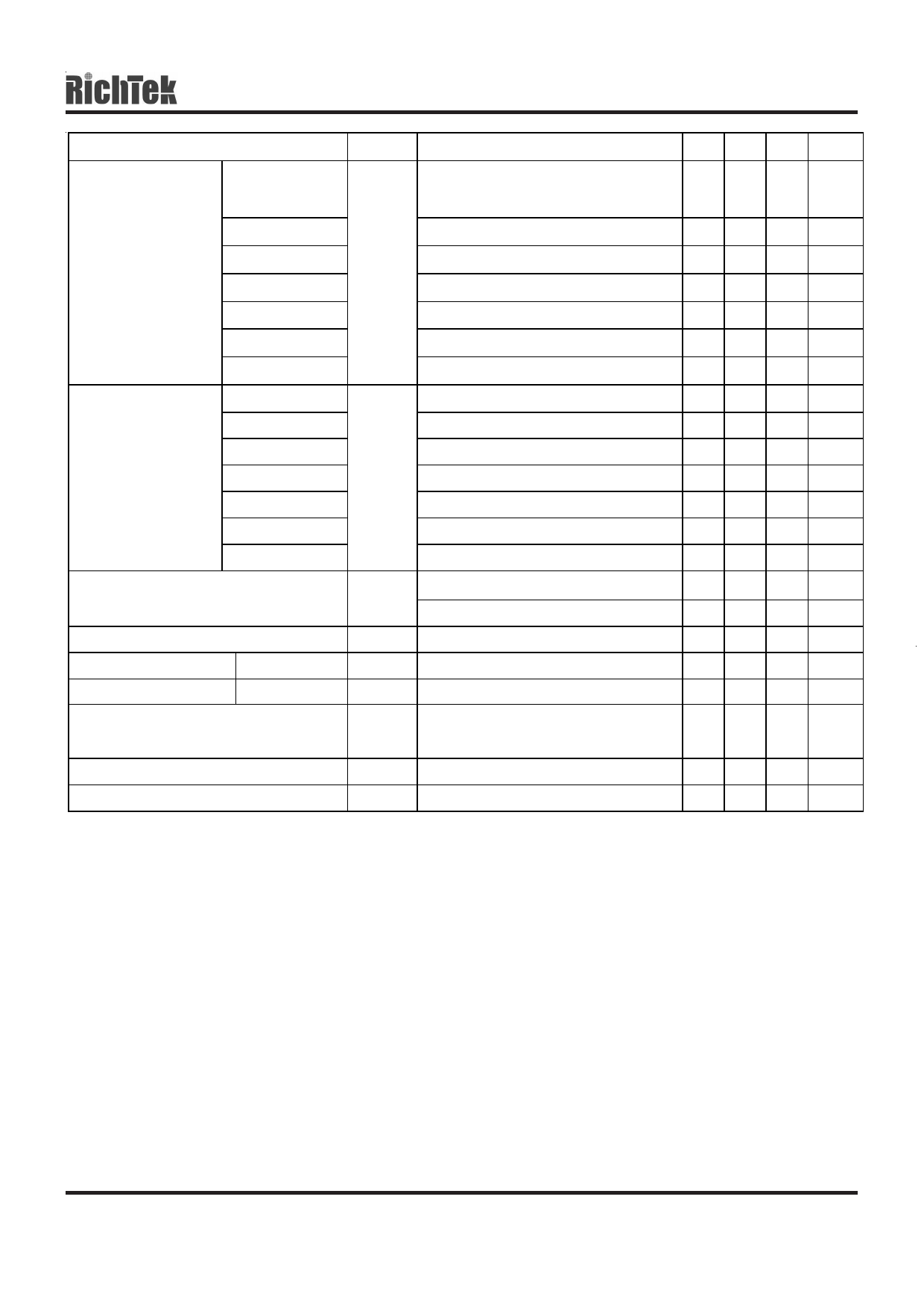
RT9164A
Parameter
Symbol
Test Conditions
Min Typ Max Units
RT9164A
IOUT = 10mA,
1.5V ≤ VIN−V OUT ≤ 10V
-- 0.1 0.3 %
RT9164A -15
I OUT = 0mA, 3.3V ≤ VIN ≤ 15V
-- 1 6 mV
Line Regulation (4)
RT9164A -18
RT9164A -25
∆VLINE
I OUT = 0mA, 3.3V ≤ VIN ≤ 15V
I OUT = 0mA, 4.0V ≤ VIN ≤ 15V
-- 1 6 mV
-- 1 6 mV
RT9164A -28
I OUT = 0mA, 4.25V ≤ VIN ≤ 15V
-- 1 6 mV
RT9164A -33
I OUT = 0mA, 4.75V ≤ VIN ≤ 15V
-- 1 6 mV
RT9164A -35
I OUT = 0mA, 5.0V ≤ VIN ≤ 15V
-- 1 6 mV
RT9164A
(VIN−VOUT) = 3V, 0mA ≤ I OUT ≤ 1.0A -- 0.2 0.4 %
Load Regulation (4)
RT9164A -15
RT9164A -18
RT9164A -25
RT9164A -28
RT9164A -33
∆VLOAD
VIN = 3.3V, 0 ≤ I OUT ≤ 1.0A
VIN = 3.3V, 0 ≤ I OUT ≤ 1.0A
VIN = 4.0V, 0 ≤ I OUT ≤ 1.0A
VIN = 4.25V, 0 ≤ I OUT ≤ 1.0A
VIN = 4.75V, 0 ≤ I OUT ≤ 1.0A
-- 1 10 mV
-- 1 10 mV
-- 1 10 mV
-- 1 10 mV
-- 1 12 mV
Dropout Voltage (5)
RT9164A -35
VDROP
VIN = 5.0V, 0 ≤ I OUT ≤ 1.0A
I OUT = 500mA
I OUT = 1.0A
-- 1 15 mV
-- 1.15 1.25 V
-- 1.3 1.4 V
Current Limit
Minimum Load Current RT9164A
ILIMIT
VIN = 5V
(VIN−VOUT) = 2V
1.0 1.8 --
A
-- 5 10 mA
Quiescent Current
RT9164A -XX IQ
VIN = 5V
-- 5 10 mA
Ripple Rejection
PSRR
fRIPPLE = 120Hz ,
(VIN − VOUT) = 2V, VRIPPLE = 1VP-P
-- 72 -- dB
Adjust Pin Current
IADJ
-- 65 120 µA
Adjust Pin Current Change
∆IADJ 10mA ≤ IOUT ≤ 1.0A, VIN = 5V
-- 0.2 5 µA
Note 1. Stresses beyond those listed under “Absolute Maximum Ratings” may cause permanent damage to the device.
These are stress ratings only, and functional operation of the device at these or any other conditions beyond those
indicated in the operational sections of the specifications is not implied. Exposure to absolute maximum rating
conditions for extended periods may affect device reliability.
Note 2. Devices are ESD sensitive. Handling precaution recommended. The human body model is a 100pF capacitor
discharged through a 1.5KΩ resistor into each pin.
Note 3. The device is not guaranteed to function outside its operating conditions.
Note 4. Low duty cycle pulse testing with Kelvin connections.
Note 5. Dropout voltage is defined as the input to output differential at which the output voltage drops 1% below the value
measured with a 2V differential.
DS9164A-01 December 2003
www.richtek.com
5
Share Link: 