PI74ALVCH16835 Ver la hoja de datos (PDF) - Pericom Semiconductor
Número de pieza
componentes Descripción
Fabricante
PI74ALVCH16835 Datasheet PDF : 5 Pages
| |||
PI74ALVCH16835
1122334455667788990011223344556677889900112233445566778899001122112233445566778899001122334455667788990011223344556677889900112211223344556677889900112233445566778899001122334455667788990011221122334455667788990011223344556677889900112233445566778899001122112233445566778899001122
18-Bit Universal Bus Driver
with 3-STATE Outputs
Product Features
• PI74ALVCH16835 is designed for low voltage operation
• VCC = 2.3V to 3.6V
• Hysteresis on all inputs
• Typical VOLP (Output Ground Bounce)
< 0.8V at VCC = 3.3V, TA = 25°C
• Typical VOHV (Output VOH Undershoot)
< 2.0V at VCC = 3.3V, TA = 25°C
• Bus Hold retains last active bus state during 3-STATE,
eliminating the need for external pullup resistors
• Industrial operation at 40°C to +85°C
• Packages available:
56-pin 240 mil wide plastic TSSOP (A)
56-pin 300 mil wide plastic SSOP (V)
56-pin 173 mil wide plastic TVSOP (K)
Product Description
Pericom Semiconductor’s PI74ALVCH series of logic circuits are
produced in the Company’s advanced 0.5 micron CMOS technology,
achieving industry leading speed.
The 18-bit PI74ALVCH16835 universal bus driver is designed for
2.3V to 3.6V Vcc operation.
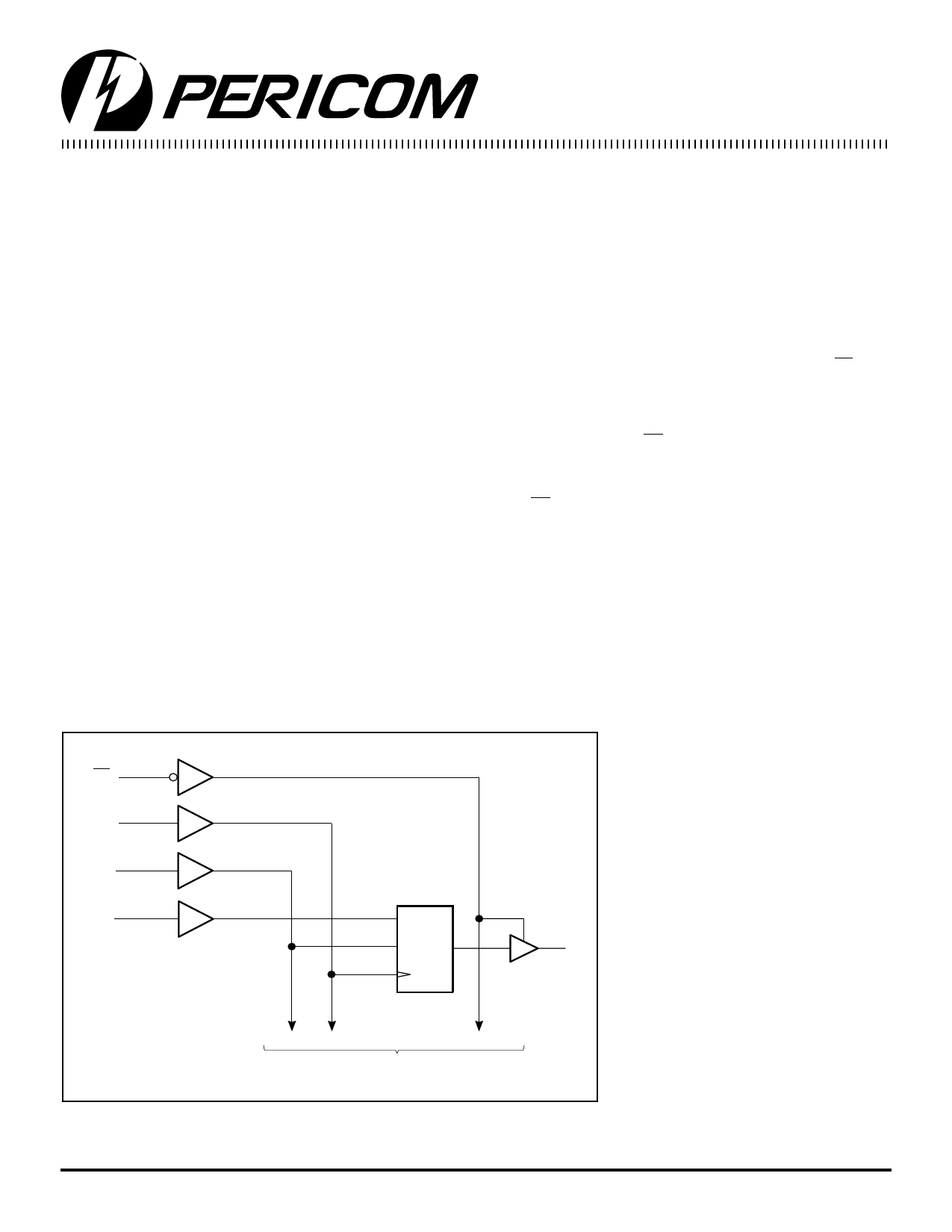
Data flow from A to Y is controlled by Output Enable (OE). The
device operates in the transparent mode when LE is HIGH. The A
data is latched if CLK is held at a high or low logic level. If LE is
LOW, the A-bus is stored in the latch/flip-flop on the low-to-high
transition of CLK. When OE is HIGH, the outputs are in the high-
impedance state.
To ensure the high-impedance state during power up or power
down, OE should be tied to Vcc through a pullup resistor; the
minimum value of the resistor is determined by the current-sinking
capability of the driver.
Active bus-hold circuitry is provided to hold unused or floating
data inputs at a valid logic level.
Logic Block Diagram
27
OE
30
CLK
28
LE
54
A1
1D
C1
CLK
3 Y1
TO 17 OTHER CHANNELS
1
PS8169A 07/30/98
Share Link: 