TEFT4300 Ver la hoja de datos (PDF) - Vishay Semiconductors
Número de pieza
componentes Descripción
Fabricante
TEFT4300 Datasheet PDF : 5 Pages
| |||
www.vishay.com
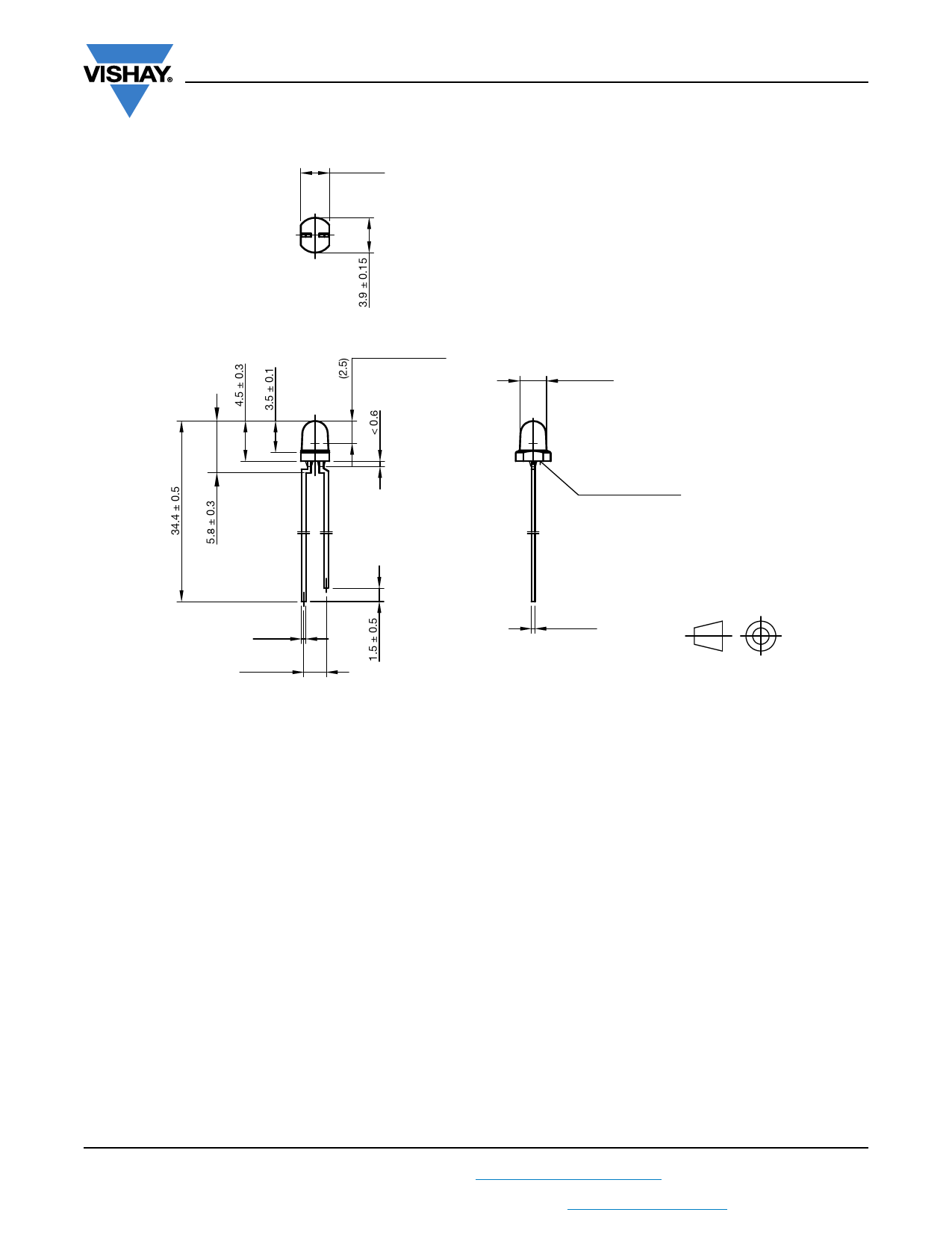
PACKAGE DIMENSIONS in millimeters
3.2 ± 0.1
E
C
CHIP POSITION
TEFT4300
Vishay Semiconductors
Ø 3 ± 0.1
AREA NOT PLANE
+ 0.2
0.5 - 0.1
2.54 nom.
Drawing-No.: 6.544-5269.01-4
Issue: 6; 28.07.14
+ 0.15
0.4 - 0.05
technical drawings
according to DIN
specifications
Rev. 1.7, 04-Aug-14
4
Document Number: 81549
For technical questions, contact: detectortechsupport@vishay.com
THIS DOCUMENT IS SUBJECT TO CHANGE WITHOUT NOTICE. THE PRODUCTS DESCRIBED HEREIN AND THIS DOCUMENT
ARE SUBJECT TO SPECIFIC DISCLAIMERS, SET FORTH AT www.vishay.com/doc?91000
Share Link: 