HI-200 Ver la hoja de datos (PDF) - Renesas Electronics
Número de pieza
componentes Descripción
Fabricante
HI-200 Datasheet PDF : 11 Pages
| |||
HI-200, HI-201
Dual/Quad SPST, CMOS Analog Switches
HI-200/HI-201 (dual/quad) are monolithic devices comprising
independently selectable SPST switches which feature fast
switching speeds (HI-200 240ns, and HI-201 185ns)
combined with low power dissipation (15mW at 25oC). Each
switch provides low “ON” resistance operation for input signal
voltage up to the supply rails and for signal current up to
80mA. Rugged DI construction eliminates latch-up and
substrate SCR failure modes.
All devices provide break-before-make switching and are
TTL and CMOS compatible for maximum application
versatility. HI-200/HI-201 are ideal components for use in
high frequency analog switching. Typical applications
include signal path switching, sample and hold circuit, digital
filters, and operational amplifier gain switching networks.
Ordering Information
TEMP.
PART NUMBER RANGE (°C)
PACKAGE
PKG.
DWG. #
HI3-0200-5Z
(Note) (No
longer available
or supported)
0 to 75
14 Ld PDIP*
(Pb-free)
E14.3
HI1-0201-2
-55 to 125 16 Ld CERDIP F16.3
HI3-0201-5Z
(Note)
0 to 75
16 Ld PDIP*
(Pb-free)
E16.3
HI4P0201-5Z
(Note) (No
longer available
or supported)
0 to 75
20 Ld PLCC
(Pb-free)
N20.35
HI9P0201-5Z
(Note)
0 to 75
16 Ld SOIC
(Pb-free)
M16.15
HI9P0201-9Z
(Note)
-40 to 85
16 Ld SOIC
(Pb-free)
M16.15
*Pb-free PDIPs can be used for through hole wave solder
processing only. They are not intended for use in Reflow solder
processing applications.
NOTE: Intersil Pb-free products employ special Pb-free material sets;
molding compounds/die attach materials and 100% matte tin plate ter-
mination finish, which are RoHS compliant and compatible with both
SnPb and Pb-free soldering operations. Intersil Pb-free products are
MSL classified at Pb-free peak reflow temperatures that meet or ex-
ceed the Pb-free requirements of IPC/JEDEC J STD-020. Pb-free
PDIPs can be used for through hole wave solder processing only. They
are not intended for use in Reflow solder processing applications.
DATASHEET
FN3121
Rev 9.00
September 15, 2015
Features
• Pb-Free Available (RoHS Compliant)
• Analog Voltage Range . . . . . . . . . . . . . . . . . . . . . . . 15V
• Analog Current Range . . . . . . . . . . . . . . . . . . . . . . . 80mA
• Turn-On Time . . . . . . . . . . . . . . . . . . . . . . . . . . . . . . 240ns
• Low rON . . . . . . . . . . . . . . . . . . . . . . . . . . . . . . . . . . . 55
• Low Power Dissipation . . . . . . . . . . . . . . . . . . . . . . .15mW
• TTL/CMOS Compatible
Applications
• High Frequency Analog Switching
• Sample and Hold Circuits
• Digital Filters
• Operational Amplifier Gain Switching Networks
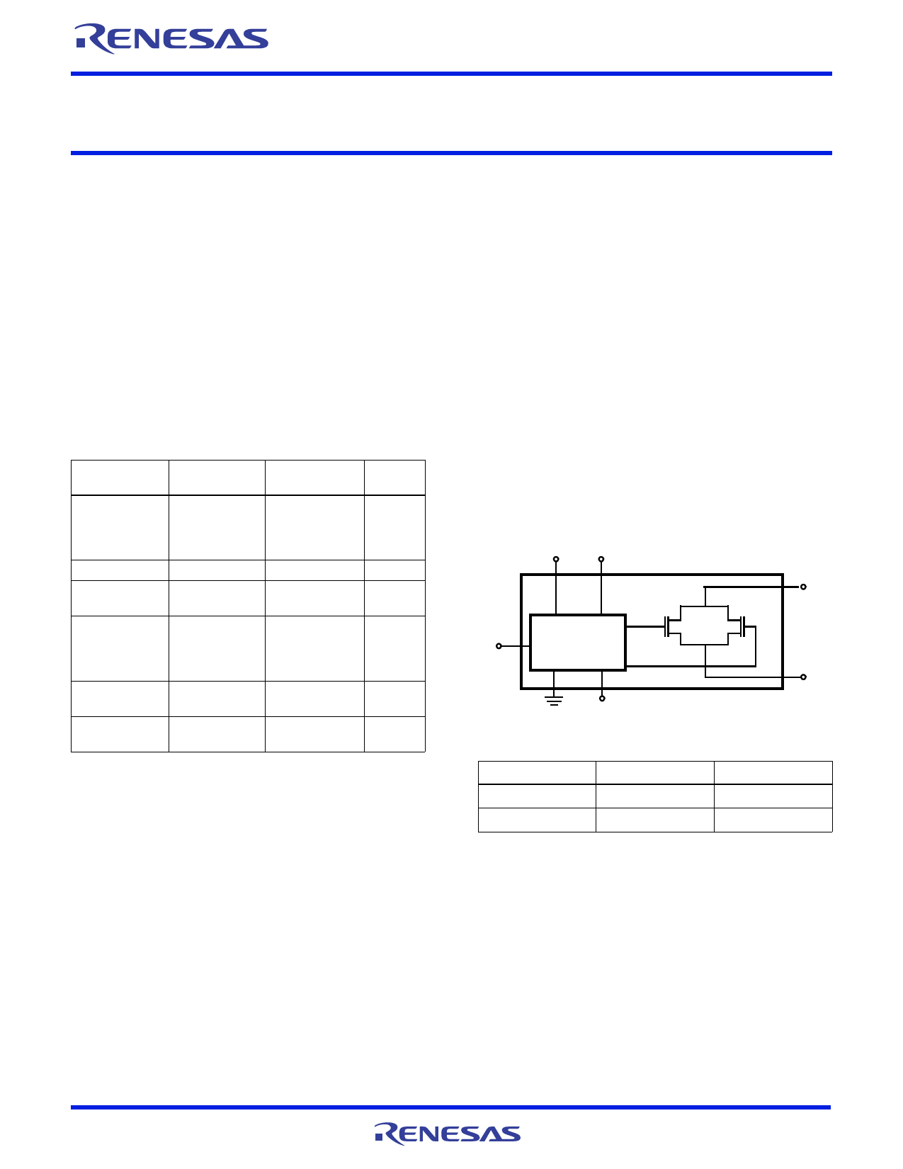
Functional Diagram
V+
VREF
LOGIC
INPUT
REFERENCE,
LEVEL SHIFTER,
AND DRIVER
GATE
INPUT
SOURCE
SWITCH
CELL
GATE
DRAIN
OUTPUT
V-
LOGIC
0
1
TRUTH TABLE
HI-200
ON
OFF
HI-201
ON
OFF
FN3121 Rev 9.00
September 15, 2015
Page 1 of 11
Share Link: 