MC100EL38(2008) Ver la hoja de datos (PDF) - ON Semiconductor
NГәmero de pieza
componentes DescripciГіn
Fabricante
MC100EL38 Datasheet PDF : 8 Pages
| |||
MC100EL38
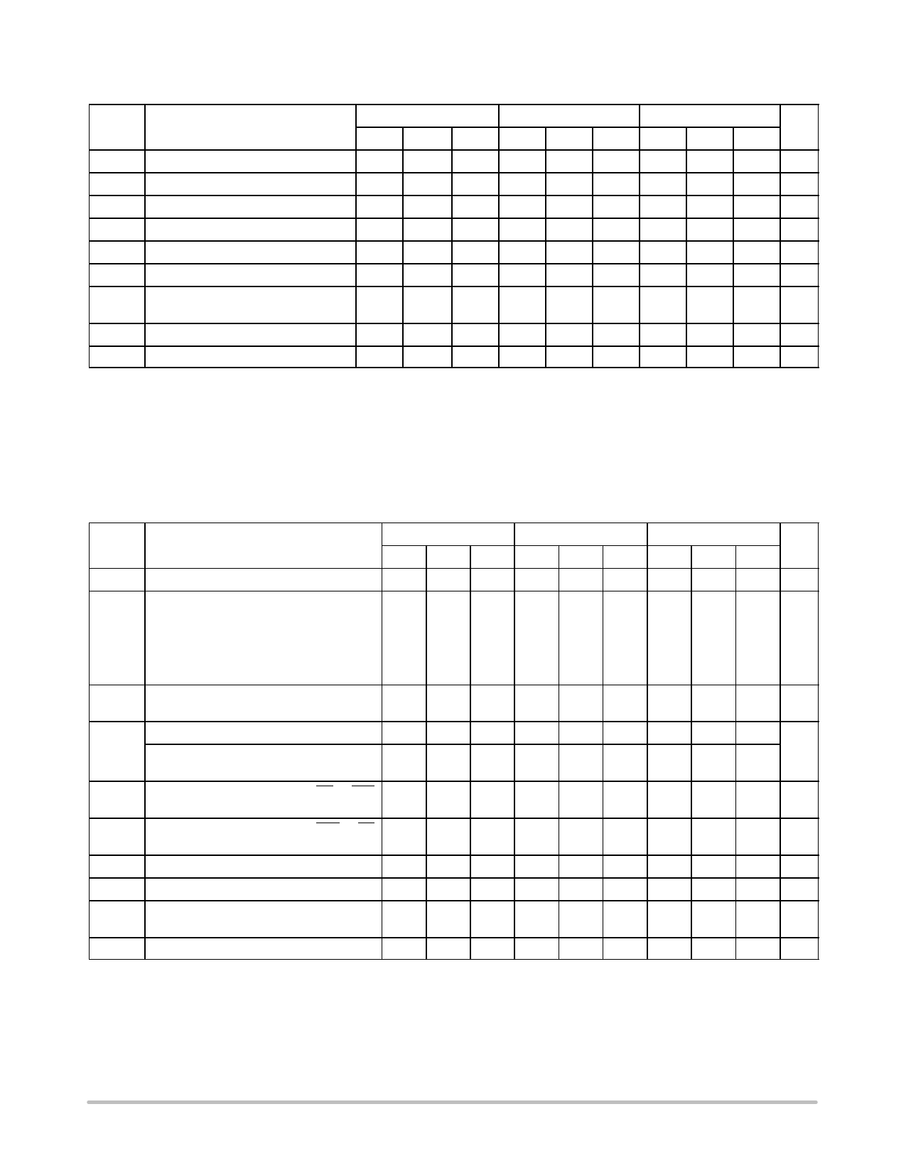
Table 5. 100EL SERIES NECL DC CHARACTERISTICS VCC = 0.0 V; VEE = вҲ’5.0 V (Note 4)
вҲ’40В°C
25В°C
85В°C
Symbol
Characteristic
Min Typ Max Min Typ Max Min Typ Max Unit
IEE
VOH
VOL
VIH
VIL
VBB
VIHCMR
Power Supply Current
Output HIGH Voltage (Note 5)
Output LOW Voltage (Note 5)
Input HIGH Voltage (SingleвҲ’Ended)
Input LOW Voltage (SingleвҲ’Ended)
Output Voltage Reference
Input HIGH Voltage Common Mode
Range (Differential) (Note 6)
50
60
50
60
54
65 mA
вҲ’1085 вҲ’1005 вҲ’880 вҲ’1025 вҲ’955 вҲ’880 вҲ’1025 вҲ’955 вҲ’880 mV
вҲ’1830 вҲ’1695 вҲ’1555 вҲ’1810 вҲ’1705 вҲ’1620 вҲ’1810 вҲ’1705 вҲ’1620 mV
вҲ’1165
вҲ’880 вҲ’1165
вҲ’880 вҲ’1165
вҲ’880 mV
вҲ’1810
вҲ’1475 вҲ’1810
вҲ’1475 вҲ’1810
вҲ’1475 mV
вҲ’1.38
вҲ’1.26 вҲ’1.38
вҲ’1.26 вҲ’1.38
вҲ’1.26 V
вҲ’3.35
вҲ’0.55 вҲ’3.35
вҲ’0.55 вҲ’3.35
вҲ’0.55 V
IIH
Input HIGH Current
IIL
Input LOW Current
150
150
150 mA
0.5
0.5
0.5
mA
NOTE: Device will meet the specifications after thermal equilibrium has been established when mounted in a test socket or printed circuit
board with maintained transverse airflow greater than 500 lfpm. Electrical parameters are guaranteed only over the declared
operating temperature range. Functional operation of the device exceeding these conditions is not implied. Device specification limit
values are applied individually under normal operating conditions and not valid simultaneously.
4. Input and output parameters vary 1:1 with VCC. VEE can vary +0.8 V / вҲ’0.5 V.
5. Outputs are terminated through a 50 W resistor to VCC вҲ’ 2.0 V.
6. VIHCMR min varies 1:1 with VEE, VIHCMR max varies 1:1 with VCC. The VIHCMR range is referenced to the most positive side of the differential input
signal. Normal operation is obtained if the HIGH level falls within the specified range and the peak-to-peak voltage lies between VPPmin and 1 V.
Table 6. AC CHARACTERISTICS VCC = 5.0 V; VEE = 0.0 V or VCC = 0.0 V; VEE = вҲ’5.0 V (Note 7)
вҲ’40В°C
25В°C
85В°C
Symbol
Characteristic
Min Typ Max Min Typ Max Min Typ Max Unit
fmax
Maximum Toggle Frequency
TBD
TBD
TBD
GHz
tPLH
Propagation Delay to Output
tPHL
CLK вҶ’ Q (Differential) 810
CLK вҶ’ Q (SingleвҲ’Ended) 710
CLK вҶ’ Phase_Out (Differential) 800
CLK вҶ’ Phase_Out (SingleвҲ’Ended) 750
MR вҶ’ Q 510
1010 850
1010 750
1000 840
1050 790
810 540
1050 900
1050 800
1040 890
1090 840
840 570
ps
1100
1100
1090
1140
870
tSKEW Within-Device Skew (Note 8)
Q0 вҲ’ Q3
50
50
50 ps
All
75
75
75
tJITTER
CycleвҲ’toвҲ’Cycle Jitter
Part-to-Part
Q0 вҲ’ Q3 (Differential)
All
TBD
200
240
TBD
200
240
TBD
ps
200
240
tS
Setup Time
EN вҶ’ CLK
150
150
150
ps
DIVSEL вҶ’ CLK
tH
Hold Time
CLK вҶ’ EN
150
150
150
ps
CLK вҶ’ Div_Sel
200
200
200
VPP
Input Swing (Note 9)
tRR
Reset Recovery Time
tPW
Minimum Pulse Width
150
CLK 800
MR 700
1000 150
100
800
700
1000 150
100
800
700
1000 mV
100 ps
ps
tr, tf
Output Rise/Fall Times Q (20% вҲ’ 80%)
280
550 280
550 280
550 ps
NOTE: Device will meet the specifications after thermal equilibrium has been established when mounted in a test socket or printed circuit
board with maintained transverse airflow greater than 500 lfpm. Electrical parameters are guaranteed only over the declared
operating temperature range. Functional operation of the device exceeding these conditions is not implied. Device specification limit
values are applied individually under normal operating conditions and not valid simultaneously.
7. VEE can vary +0.8 V / вҲ’0.5 V.
8. Skew is measured between outputs under identical transitions.
9. VPP(min) is minimum input swing for which AC parameters guaranteed. The device has a DC gain of вүҲ40.
http://onsemi.com
4
Share Link: 