LC36256AL Ver la hoja de datos (PDF) - SANYO -> Panasonic
NГәmero de pieza
componentes DescripciГіn
Fabricante
LC36256AL Datasheet PDF : 7 Pages
| |||
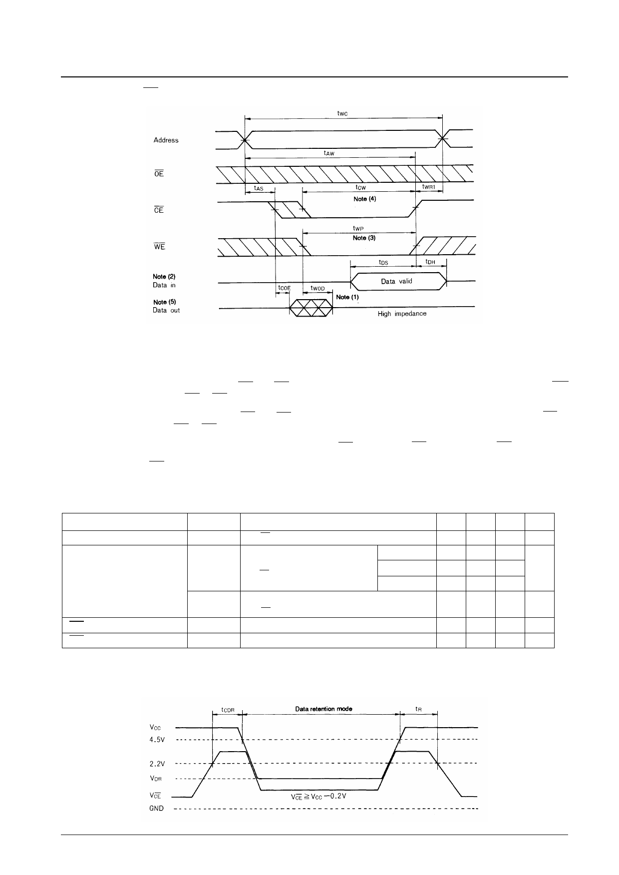
вҖў Write Cycle (2): CE Control Note (6)
LC36256AL, AML-70/85/10/12
Notes (1) tCOD, tOOD, and tWOD are defined as the time at which the outputs becomes the high impedance state and
are not referred to output voltage levels.
(2) An external antiphase signal must not be applied when DOUT is in the output state.
(3) tWP is the time interval that CE and WE are low-level and is defined as the interval from the falling of WE
to the rising of CE or WE whichever is earlier.
(4) tCW is the time interval that CE and WE are low-level and is defined as the time from the falling of CE to
the rising of CE or WE whichever is earlier.
(5) DOUT goes to the high-impedance state when either OE is high-level, CE is high-level, or WE is low-level.
(6) When OE is high-level during the write cycle, DOUT goes to the high-impedance state.
Data Retention Characteristics at Ta = 0 to +70В°C
Parameter
Data retention supply voltage
Symbol
VDR
Conditions
VCE вүҘ VCCвҖ“0.2V
Data retention supply current
ICCDR1
ICCDR2
CE setup time
tCDR
CE hold time
tR
* Reference values at VCC = 5V, Ta = 25В°C
VCC = 3.0V,
VCE вүҘ 2.8V
VCC = 2.0 to 5.5V,
VCE вүҘ VCCвҖ“0.2V
** tRC = Read Cycle time
Data Retention Waveform
min typ* max Unit
2.0
5.5
V
0 to +70В°C
10
0 to +40В°C
2 ВөA
25В°C
0.25 1
0.5 25 ВөA
0
ns
tRC**
ns
No. 4163-6/7
Share Link: 