CAT28C257 Ver la hoja de datos (PDF) - ON Semiconductor
Número de pieza
componentes Descripción
Fabricante
CAT28C257 Datasheet PDF : 13 Pages
| |||
CAT28C257
Table 8. A.C. CHARACTERISTICS, WRITE CYCLE (VCC = 5 V ±10%, unless otherwise specified.)
28C257−12
28C257−15
Symbol
Parameter
Min
Typ
Max
Min
Typ
Max
Units
tWC
Write Cycle Time
5
5
ms
tAS
Address Setup Time
0
0
ns
tAH
Address Hold Time
50
50
ns
tCS
CE Setup Time
0
0
ns
tCH
CE Hold Time
0
0
ns
tCW (Note 10)
CE Pulse Time
100
100
ns
tOES
OE Setup Time
0
0
ns
tOEH
OE Hold Time
0
0
ns
tWP (Note 10)
WE Pulse Width
100
100
ns
tDS
Data Setup Time
50
50
ns
tDH
Data Hold Time
0
0
ns
tINIT (Note 11)
Write Inhibit Period After Power−up
5
10
5
10
ms
tBLC (Notes 11, 12) Byte Load Cycle Time
0.1
100
0.1
100
ms
10. A write pulse of less than 20 ns duration will not initiate a write cycle.
11. This parameter is tested initially and after a design or process change that affects the parameter.
12. A timer of duration tBLC max. begins with every LOW to HIGH transition of WE. If allowed to time out, a page or byte write will begin; however
a transition from HIGH to LOW within tBLC max. stops the timer.
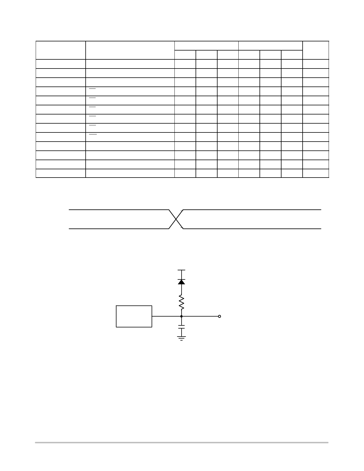
VCC − 0.3 V
0.0 V
INPUT PULSE LEVELS
2.0 V
0.8 V
REFERENCE POINTS
Figure 2. A.C. Testing Input/Output Waveform (Note 13)
13. Input rise and fall times (10% and 90%) < 10 ns.
1.3 V
1N914
DEVICE
UNDER
TEST
3.3 K
CL = 100 pF
OUT
CL INCLUDES JIG CAPACITANCE
Figure 3. A.C. Testing Load Circuit (example)
http://onsemi.com
5
Share Link: 