ISL84516IB Ver la hoja de datos (PDF) - Renesas Electronics
Número de pieza
componentes Descripción
Fabricante
ISL84516IB Datasheet PDF : 10 Pages
| |||
ISL84516, ISL84517
Absolute Maximum Ratings
V+ to V- . . . . . . . . . . . . . . . . . . . . . . . . . . . . . . . . . . . . . -0.3 to 15V
Input Voltages
IN (Note 2). . . . . . . . . . . . . . . . . . . . . ((V-) - 0.3V) to ((V+) + 0.3V)
NO, NC (Note 2) . . . . . . . . . . . . . . . . ((V-) - 0.3V) to ((V+) + 0.3V)
Output Voltages
COM (Note 2) . . . . . . . . . . . . . . . . . . ((V-) - 0.3V) to ((V+) + 0.3V)
Continuous Current (Any Terminal) . . . . . . . . . . . . . . . . . . . . . 20mA
Peak Current NO, NC, or COM
(Pulsed 1ms, 10% Duty Cycle, Max) . . . . . . . . . . . . . . . . . . 30mA
ESD Rating (Per MIL-STD-883 Method 3015). . . . . . . . . . . . . >2kV
Thermal Information
Thermal Resistance (Typical, Note 3)
JA (oC/W)
5 Ld SOT-23 Package . . . . . . . . . . . . . . . . . . . . . . .
225
8 Ld SOIC Package . . . . . . . . . . . . . . . . . . . . . . . . .
170
Maximum Junction Temperature (Plastic Package) . . . . . . . 150oC
Moisture Sensitivity (See Technical Brief TB363)
All Packages . . . . . . . . . . . . . . . . . . . . . . . . . . . . . . . . . . . Level 1
Maximum Storage Temperature Range. . . . . . . . . . . . -65oC to 150oC
Maximum Lead Temperature (Soldering 10s) . . . . . . . . . . . . 300oC
(Lead Tips Only)
Operating Conditions
Temperature Range
ISL8451XIX . . . . . . . . . . . . . . . . . . . . . . . . . . . . . . . . -40oC to 85oC
CAUTION: Stresses above those listed in “Absolute Maximum Ratings” may cause permanent damage to the device. This is a stress only rating and operation of the
device at these or any other conditions above those indicated in the operational sections of this specification is not implied.
NOTES:
2. Signals on NO, NC, COM, or IN exceeding V+ or V- are clamped by internal diodes. Limit forward diode current to maximum current ratings.
3. JA is measured with the component mounted on a low effective thermal conductivity test board in free air. See Tech Brief TB379 for details.
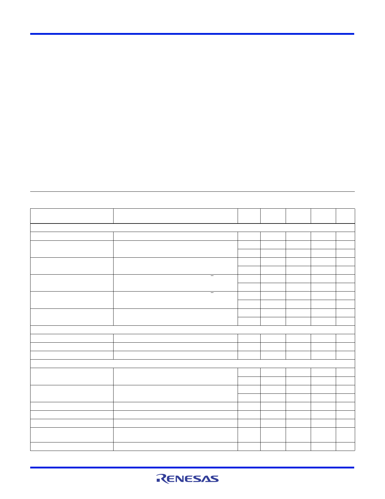
Electrical Specifications - 5V Supply Test Conditions: VSUPPLY = 4.5V to 5.5V, VINH = 3.5V, VINL = 1.5V (Note 4),
Unless Otherwise Specified
PARAMETER
TEST CONDITIONS
TEMP (NOTE 5)
(NOTE 5)
(oC)
MIN
TYP
MAX UNITS
ANALOG SWITCH CHARACTERISTICS
Analog Signal Range, VANALOG
ON Resistance, RON
VS = 5V, ICOM = 1.0mA, VCOM = 3V
(See Figure 4)
Full
V-
-
V+
V
25
-
13
20
Full
-
-
25
RON Flatness, RFLAT(ON)
VS = 5V, ICOM = 1.0mA, VCOM = -3V, 0V, 3V
25
-
3
4
Full
-
4
6
NO or NC OFF Leakage Current,
INO(OFF) or INC(OFF)
VS = 5.5V, VCOM = 4.5V, VNO or VNC = +4.5V
(Note 6)
25
-1
0.01
Full
-20
-
1
nA
20
nA
COM OFF Leakage Current,
ICOM(OFF)
VS = 5.5V, VCOM = 4.5V, VNO or VNC = +4.5V
(Note 6)
25
-1
0.01
Full
-20
-
1
nA
20
nA
COM ON Leakage Current,
ICOM(ON)
VS = 5.5V, VCOM = VNO or VNC = 4.5V (Note 6)
DIGITAL INPUT CHARACTERISTICS
25
-2
Full
-40
0.01
-
2
nA
40
nA
Input Voltage High, VINH
Input Voltage Low, VINL
Input Current, IINH, IINL
DYNAMIC CHARACTERISTICS
VS = 5.5V, VIN = 0V or V+
Full (V+) - 1.5
-
V+
V
Full
V-
-
(V+) - 3.5 V
Full
-0.5
-
0.5
A
Turn-ON Time, tON
VNO or VNC = 3V, RL = 300, CL = 35pF,
VIN = 0 to V+ (See Figure 1)
25
-
Full
-
40
100
ns
-
150
ns
Turn-OFF Time, tOFF
VNO or VNC = 3V, RL = 300, CL = 35pF,
VIN = 0 to V+ (See Figure 1)
25
-
Full
-
30
75
ns
-
125
ns
Charge Injection, Q
CL = 1.0nF, VG = 0V, RG = 0 (See Figure 2)
25
-
10
20
pC
OFF Isolation
RL = 50, CL = 15pF, f = 100kHz (See Figure 3)
25
-
>86
-
dB
NO or NC OFF Capacitance, COFF f = 1MHz, VNO or VNC = VCOM = 0V (See Figure 5)
25
-
9
-
pF
COM OFF Capacitance,
CCOM(OFF)
f = 1MHz, VNO or VNC = VCOM = 0V (See Figure 5)
25
-
9
-
pF
COM ON Capacitance, CCOM(ON) f = 1MHz, VNO or VNC = VCOM = 0V (See Figure 5)
25
-
22
-
pF
FN6030 Rev.4.00
May 19, 2005
Page 3 of 10
Share Link: 