HV5308 Ver la hoja de datos (PDF) - Microchip Technology
Número de pieza
componentes Descripción
Fabricante
HV5308
Microchip Technology

HV5308 Datasheet PDF : 17 Pages
| |||
HV5308 / HV5408
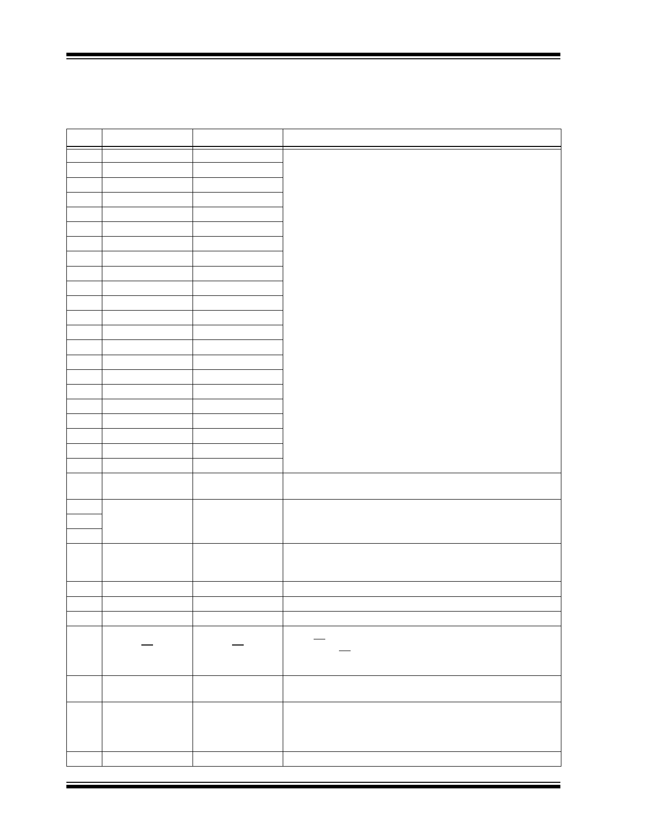
2.0 PIN DESCRIPTION
The locations of the pins are listed in Package Type.
TABLE 2-1: PIN DESCRIPTION PQFP
Pin #
HV5308
HV5408
1
HVOUT22
2
HVOUT21
3
HVOUT20
4
HVOUT19
5
HVOUT18
6
HVOUT17
7
HVOUT16
8
HVOUT15
9
HVOUT14
10
HVOUT13
11
HVOUT12
12
HVOUT11
13
HVOUT10
14
HVOUT9
15
HVOUT8
16
HVOUT7
17
HVOUT6
18
HVOUT5
19
HVOUT4
20
HVOUT3
21
HVOUT2
22
HVOUT1
HVOUT11
HVOUT12
HVOUT13
HVOUT14
HVOUT15
HVOUT16
HVOUT17
HVOUT18
HVOUT19
HVOUT20
HVOUT21
HVOUT22
HVOUT23
HVOUT24
HVOUT25
HVOUT26
HVOUT27
HVOUT28
HVOUT29
HVOUT30
HVOUT31
HVOUT32
23
DATA OUT
DATA OUT
24
25
N/C
N/C
26
27
CLK
CLK
28
GND
29
VPP
30
VDD
GND
VPP
VDD
31
LE
LE
32
DATA IN
DATA IN
33
OE
OE
34
N/C
N/C
Description
High voltage outputs.
High voltage push-pull outputs, which, depending on controlling
low voltage data, can drive loads either to GND, or to VPP rail lev-
els.
Serial data output.
Data output for cascading to the data input of the next device.
No connect.
Data shift register clock
Input are shifted into the shift register on the positive edge of the
clock.
Logic and high voltage ground
High voltage power rail.
Low voltage logic power rail.
Latch enable input.
When LE is High, shift register data is transferred into a data
latch. When LE is Low, data is latched, and new data can be
clocked into the shift register.
Serial data input.
Data needs to be present before each rising edge of the clock.
Output enable input.
When OE is Low, all HV outputs are forced into a Low state,
regardless of data in each channel. When OE is High, all HV out-
puts reflect data latched.
No connect.
DS20005425A-page 6
2015 Microchip Technology Inc.
Share Link: