LC75847T Ver la hoja de datos (PDF) - ON Semiconductor
Número de pieza
componentes Descripción
Fabricante
LC75847T Datasheet PDF : 28 Pages
| |||
LC75847T
1/3, 1/4-Duty General-Purpose
LCD Driver
Overview
The LC75847T is 1/3 duty and 1/4 duty general-purpose LCD driver that can
be used for frequency display in electronic tuners under the control of a
microcontroller. The LC75847T can drive an LCD with up to 420 segments
directly. The LC75847T can also control up to 8 general-purpose output ports.
www.onsemi.com
Features
Switching between 1/3 duty and 1/4 duty drive techniques under serial data
control.
Switching between 1/2 bias and 1/3 bias drive techniques under serial data
control.
Up to 318 segments for 1/3 duty drive and 420 segments for 1/4 duty drive
can be displayed.
Serial data input supports CCB* format communication with the system
controller.
Serial data control of the power-saving mode based backup function and all
the segments forced off function.
Serial data control of switching between the segment output port and the
general-purpose output port functions.
Serial data control of frame frequency for common and segment output
waveforms.
High generality, since display data is displayed directly without decoder
intervention.
Built-in display contrast adjustment circuit
Independent VLCD for the LCD driver block
The INH pin can force the display to the off state.
RC oscillator circuit
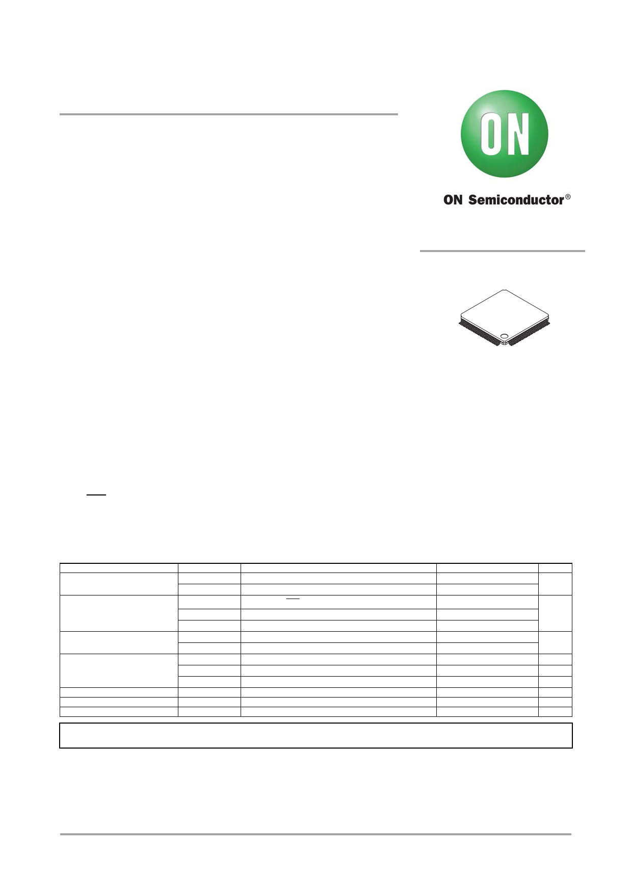
TQFP120 14x14 / TQFP120
Specifications
Absolute Maximum Ratings at Ta = 25C, VSS = 0 V
Parameter
Maximum supply voltage
Input voltage
Output voltage
Output current
Allowable power dissipation
Operating temperature
Storage temperature
Symbol
VDD max
VLCD max
VIN1
VIN2
VIN3
VOUT1
VOUT2
IOUT1
IOUT2
IOUT3
Pd max
Topr
Tstg
VDD
VLCD
Conditions
CE, CL, DI, INH
OSC
VLCD1, VLCD2
OSC
VLCD0, S1 to S106, COM1 to COM4, P1 to P8
S1 to S106
COM1 to COM4
P1 to P8
Ta = 85°C
Ratings
unit
–0.3 to +7.0
–0.3 to +7.0
V
–0.3 to +7.0
–0.3 to VDD +0.3
V
–0.3 to VLCD +0.3
–0.3 to VDD +0.3
–0.3 to VLCD +0.3
V
300
A
3 mA
5 mA
200 mW
–40 to +85
C
–55 to +125
C
Stresses exceeding those listed in the Maximum Ratings table may damage the device. If any of these limits are exceeded, device functionality should not be assumed,
damage may occur and reliability may be affected.
* Computer Control Bus (CCB) is an ON Semiconductor’s original bus format and
the bus addresses are controlled by ON Semiconductor.
ORDERING INFORMATION
See detailed ordering and shipping information on page 28 of this data sheet.
© Semiconductor Components Industries, LLC, 2017
1
July 2017 - Rev. 1
Publication Order Number :
LC75847T/D
Share Link: 