NCV8401A Ver la hoja de datos (PDF) - ON Semiconductor
Número de pieza
componentes Descripción
Fabricante
NCV8401A Datasheet PDF : 10 Pages
| |||
NCV8401A, NCV8401B
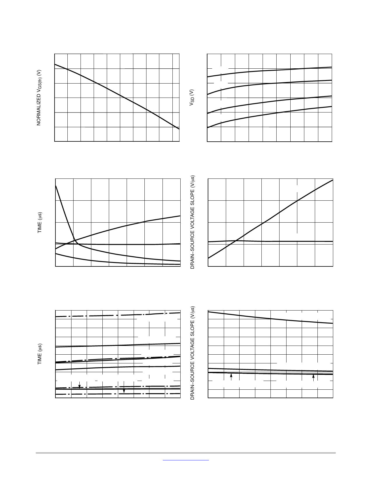
TYPICAL PERFORMANCE CURVES
1.2
1.1
1.0
0.9
0.8
0.7
0.6
−40 −20 0 20 40 60 80 100 120 140
T (°C)
Figure 14. Normalized Threshold Voltage vs.
Temperature (ID = 1.2 mA, VDS = VGS)
200
150
td(off)
100
tf
50
td(on)
tr
0
3
4
5
6
7
8
9
10
VGS (V)
Figure 16. Resistive Load Switching Time vs.
Gate−Source Voltage
(VDD = 25 V, ID = 5 A, RG = 0 W)
125
td(off), VGS = 10 V
100
td(off), VGS = 5 V
75
tf, VGS = 10 V
50
tf, VGS = 5 V
tr, VGS = 5 V
25 td(on), VGS = 5 V td(on), VGS = 10 V tr, VGS = 10 V
0
0
500
1000
1500
2000
RG (W)
Figure 18. Resistive Load Switching Time vs.
Gate Resistance (VDD = 25 V, ID = 5 A)
1.0
0.9 −40°C
0.8 25°C
0.7
100°C
0.6
150°C
0.5
0.4
1 2 3 4 5 6 7 8 9 10
IS (A)
Figure 15. Source−Drain Diode Forward
Characteristics (VGS = 0 V)
2.0
−dVDS/dt(on)
1.5
1.0
dVDS/dt(off)
0.5
0
3
4
5
6
7
8
9
10
VGS (V)
Figure 17. Resistive Load Switching
Drain−Source Voltage Slope vs. Gate−Source
Voltage (VDD = 25 V, ID = 5 A, RG = 0 W)
2.0
1.8
−dVDS/dt(on), VGS = 10 V
1.6
1.4
1.2
1.0
0.8
−dVDS/dt(on), VGS = 5 V
0.6
0.4 dVDS/dt(off), VGS = 5 V
0.2
dVDS/dt(off), VGS = 10 V
0
0
500
1000
1500
2000
RG (W)
Figure 19. Drain−Source Voltage Slope during
Turn On and Turn Off vs. Gate Resistance
(VDD = 25 V, ID = 5 A)
www.onsemi.com
6
Share Link: 