CS5205A-1 Ver la hoja de datos (PDF) - ON Semiconductor
Número de pieza
componentes Descripción
Fabricante
CS5205A-1 Datasheet PDF : 8 Pages
| |||
CS5205A−1
APPLICATIONS INFORMATION
The CS5205A−1 linear regulator provides an adjustable
voltage at currents up to 5.0 A. The regulator is protected
against short circuit, and include thermal shutdown and safe
area protection (SOA) circuitry. The SOA protection
circuitry decreases the maximum available output current as
the input−output differential voltage increases.
The CS5205A−1 has a composite PNP−NPN output
transistor and requires an output capacitor for stability. A
detailed procedure for selecting this capacitor is included in
the Stability Considerations section.
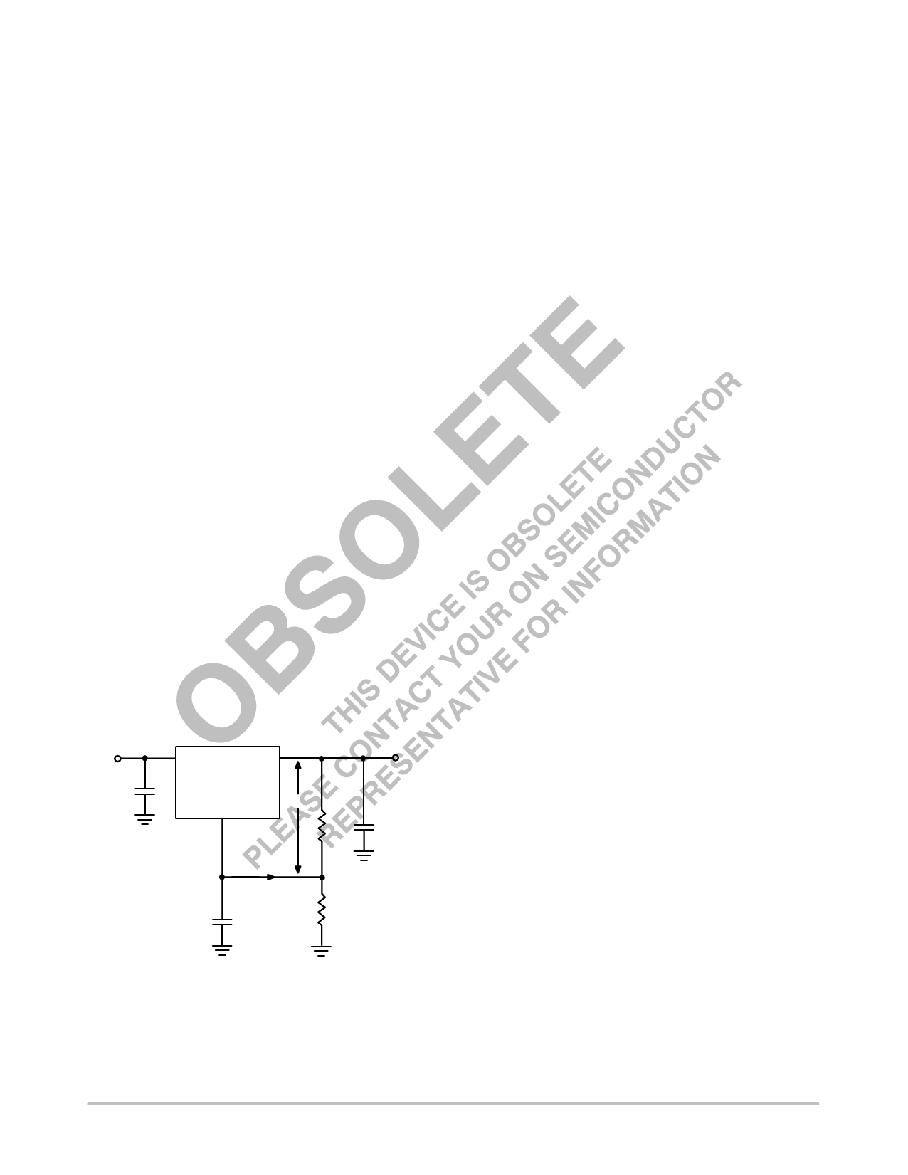
Adjustable Operation
The adjustable regulator (CS5205A−1) has an output
voltage range of 1.25 V to 13 V. An external resistor divider
sets the output voltage as shown in Figure 7. The regulator
maintains a fixed 1.25 V (typical) reference between the
output pin and the adjust pin.
A resistor divider network R1 and R2 causes a fixed
current to flow to ground. This current creates a voltage
across R2 that adds to the 1.25 V across R1 and sets the
overall output voltage. The adjust pin current (typically
50 μA) also flows through R2 and adds a small error that
should be taken into account if precise adjustment of VOUT
is necessary.
The output voltage is set according to the formula:
ǒ Ǔ VOUT + VREF
R1 ) R2
R1
) IAdj
R2
The term IAdj × R2 represents the error added by the adjust
pin current.
R1 is chosen so that the minimum load current is at least
10 mA. R1 and R2 should be the same type, e.g. metal film
for best tracking over temperature. The adjust pin is
bypassed to improve the transient response and ripple
rejection of the regulator.
VIN
C1
VIN
VOUT
CS5205A−1
Adj
VREF
R1
VOUT
C2
IAdj
R2
CAdj
Stability Considerations
The output or compensation capacitor helps determine
three main characteristics of a linear regulator: start−up
delay, load transient response and loop stability.
The capacitor value and type is based on cost, availability,
size and temperature constraints. A tantalum or aluminum
electrolytic capacitor is best, since a film or ceramic
capacitor with almost zero ESR, can cause instability. The
aluminum electrolytic capacitor is the least expensive
solution. However, when the circuit operates at low
temperatures, both the value and ESR of the capacitor will
vary considerably. The capacitor manufacturers data sheet
provides this information.
A 22 μF tantalum capacitor will work for most
applications, but with high current regulators such as the
CS5205A−1 the transient response and stability improve
with higher values of capacitor. The majority of applications
for this regulator involve large changes in load current so the
output capacitor must supply the instantaneous load current.
The ESR of the output capacitor causes an immediate drop
in output voltage given by:
DV + DI ESR
For microprocessor applications it is customary to use an
output capacitor network consisting of several tantalum and
ceramic capacitors in parallel. This reduces the overall ESR
and reduces the instantaneous output voltage drop under
load transient conditions. The output capacitor network
should be as close as possible to the load for the best results.
Protection Diodes
When large external capacitors are used with a linear
regulator it is sometimes necessary to add protection diodes.
If the input voltage of the regulator gets shorted, the output
capacitor will discharge into the output of the regulator. The
discharge current depends on the value of the capacitor, the
output voltage and the rate at which VIN drops. In the
CS5205A−1 linear regulator, the discharge path is through
a large junction and protection diodes are not usually
needed. If the regulator is used with large values of output
capacitance and the input voltage is instantaneously shorted
to ground, damage can occur. In this case, a diode connected
as shown in Figure 8 is recommended.
Figure 7. Resistor Divider Scheme for the Adjustable
Version
http://onsemi.com
4
Share Link: 