AT-41532 Ver la hoja de datos (PDF) - Avago Technologies
Número de pieza
componentes Descripción
Fabricante
AT-41532 Datasheet PDF : 14 Pages
| |||
AT-41532 Application Information
The AT-41532 is described in a low noise amplifier for use
in the 800 to 900 MHz frequency range. The amplifier is
designed for use with .032 inch thickness FR-4 printed
circuit board material.
900 MHz LNA Design
The amplifier is designed for a VCE of 5 volts and IC of 5
mA. and a minimum power supply voltage of 5.25 volts.
Higher power supply voltages will require an additional
resistance to be inserted at the power supply terminal.
The amplifier schematic is shown in Figure 16.
A component list is shown in Figure 17. The artwork
including component placement is shown in Figure 18.
C2
INPUT
L1 Q1 R6
Zo C1
L2
R1
C4 R2 R4
R3
C3 OUTPUT
L3 C4 Zo
R5
VCC = 5.25 V
C5
Figure 16. Schematic Diagram.
C1,C4
C2
C3
C5
L1
L2
L3
Q1
R1
R2
R3
R4
R5
R6
Zo
10 pF chip capacitor
Open circuited stub – see text
2.7 pF chip capacitor
1000 pF chip capacitor
8 nH chip inductor (Coilcraft 1008CS-080)
Optional (see R1)
15 nH chip inductor (Coilcraft 1008CS-150)
Avago AT-41532 Silicon Bipolar Transistor
10K Ω chip resistor (may want to substitute a
180 nH chip inductor and 50 Ω resistor for
lower noise figure , better low freq stability,
then readjust R2)
48 K Ω chip resistor (adjust for rated Ic)
3.32 K Ω chip resistor
3.32 K Ω chip resistor
51.1 Ω chip resistor
1.1K Ω chip resistor (see text)
50 Ω microstripline
Figure 17. Component Parts List.
AT-3XX32
AT-4XX32
IN
01/98 AJW
.062 FR-4
OUT
Vcc
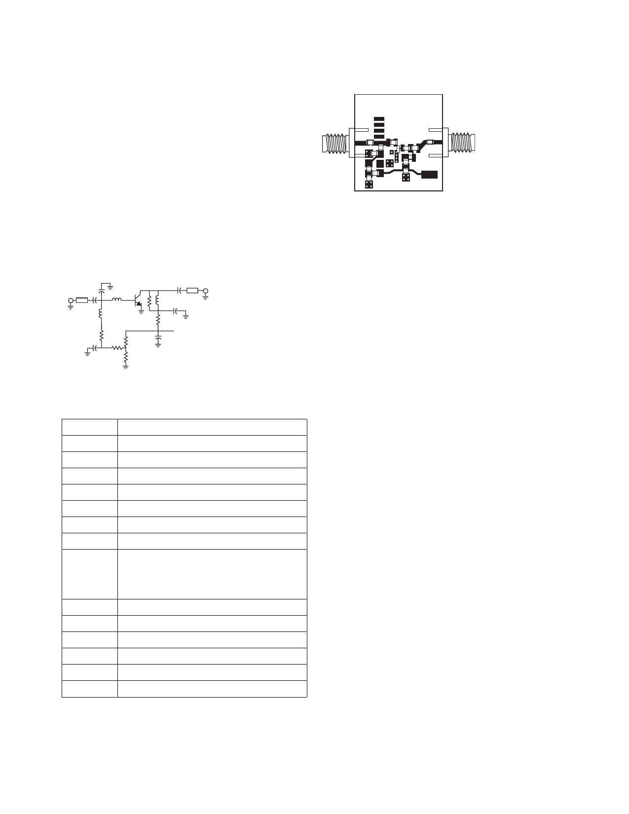
Figure 18. 1X Artwork showing Component Placement.
The input matching network uses a series inductor for the
noise match. Some fine tuning for lowest noise figure and
improved input VSWR can be accomplished by adding
capacitance at C2. The shunt C is accomplished with an
open circuited stub while a chip inductor is used for the
series element. The output impedance matching network
is a high pass structure consisting of a series capacitor and
shunt inductor. A resistor is paralleled across the shunt
inductor to enhance broad band stability through 10 GHz.
Bias insertion is accomplished through the use of the
shunt inductor appropriately bypassed. Surface mount
Coilcraft inductors were chosen for their small size.
Biasing
The bias network is designed for a nominal power supply
voltage of 5.25 volts. Resistors R1 and R2 are used to
adjust collector current. Resistor R4 can be attached to the
junction of R5 and C5 to improve bias point stability.
11
Share Link: 