M-8888-01SM Ver la hoja de datos (PDF) - Clare Inc => IXYS
Número de pieza
componentes Descripción
Fabricante
M-8888-01SM Datasheet PDF : 14 Pages
| |||
M-8888
AC Characteristics (Continued)
Parameter
Symbol
Min
DTMF Clock
Crystal clock frequency
Clock input rise time (external clock)
Clock input fall time (external clock)
Clock input duty cycle (external clock)
Capacitive load, OSC2
fC
tLHCL
tHLCL
DCCL
CLO
3.5759
-
-
40
-
Voltages referenced to VSS unless otherwise noted. VDD = 5.0V ± 5%; VSS = 0 V; fC = 3.579545 MHz; TA = -40°C to +85°C
*Typical values are for use as design aids only and are not guaranteed or subject to production testing.
Notes:
1. dBm = decibels above or below a reference power of 1 mW into a 600 Ω load.
2. Digit sequence consists of all 16 DTMF tones.
3. Tone duration = 40 ms. Tone pause = 40 ms.
4. Nominal DTMF frequencies are used.
5. Both tones in the composite signal have an equal amplitude.
6. The tone pair is deviated by ± 1.5% ± 2 Hz.
7. Bandwidth limited (3 kHz) Gaussian noise.
8. The precise dial tone frequencies are 350 and 440 Hz (± 2%).
9. For an error rate of less than 1 in 10,000.
10. Referenced to the lowest amplitude tone in the DTMF signal.
11. Referenced to the minimum valid accept level.
Typ*
3.5795
-
-
50
-
Max
3.5831
110
100
60
30
Units
MHz
ns
ns
%
pF
Electrical Characteristics - Gain Setting Amplifier
Parameter
Symbol
Min
Input leakage current (VSS ≤ VIN ≤ VDD)
Input resistance
Input offset voltage
Power supply rejection (1 KHz)
IIN
-
RIN
-
VOS
-
PSRR
-
Common mode rejection (-3.0 V≤ VIN ≤ 3.0V)
DC open-loop voltage gain
Unity gain bandwidth
CMRR
-
AVOL
-
BW
-
Output voltage swing (RL ≥ 100 KΩ to VSS)
Maximum capcitive load, GS
Maximum resistive load, GS
Common mode range (no load)
VO
-
CL
-
RL
-
VCM
-
All voltages referenced to VSS unless otherwise noted. VDD = 5.0V ± 5%; VSS = 0 V; fC = 3.579545 MHz; TA = -40°C to +85°C
*Typical values are for use as design aids only, and are not guaranteed or subject to production testing.
Typ*
100
10
25
60
60
65
1.5
4.5
100
50
3.0
Max
-
-
-
-
-
-
-
-
-
-
-
Units
nA
MΩ
mV
dB
dB
dB
MHz
VPP
pF
kΩ
VPP
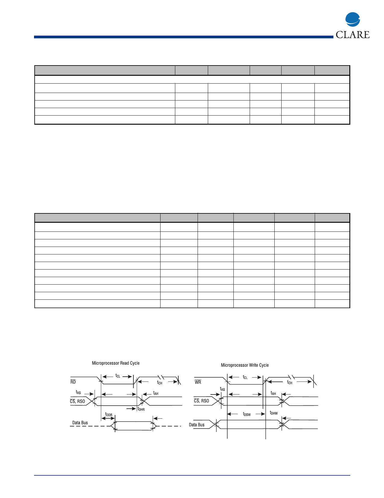
Timing Diagrams
10
www.clare.com
Rev. 1
Share Link: 