CXD2588R Ver la hoja de datos (PDF) - Sony Semiconductor
Número de pieza
componentes Descripción
Fabricante
CXD2588R Datasheet PDF : 121 Pages
| |||
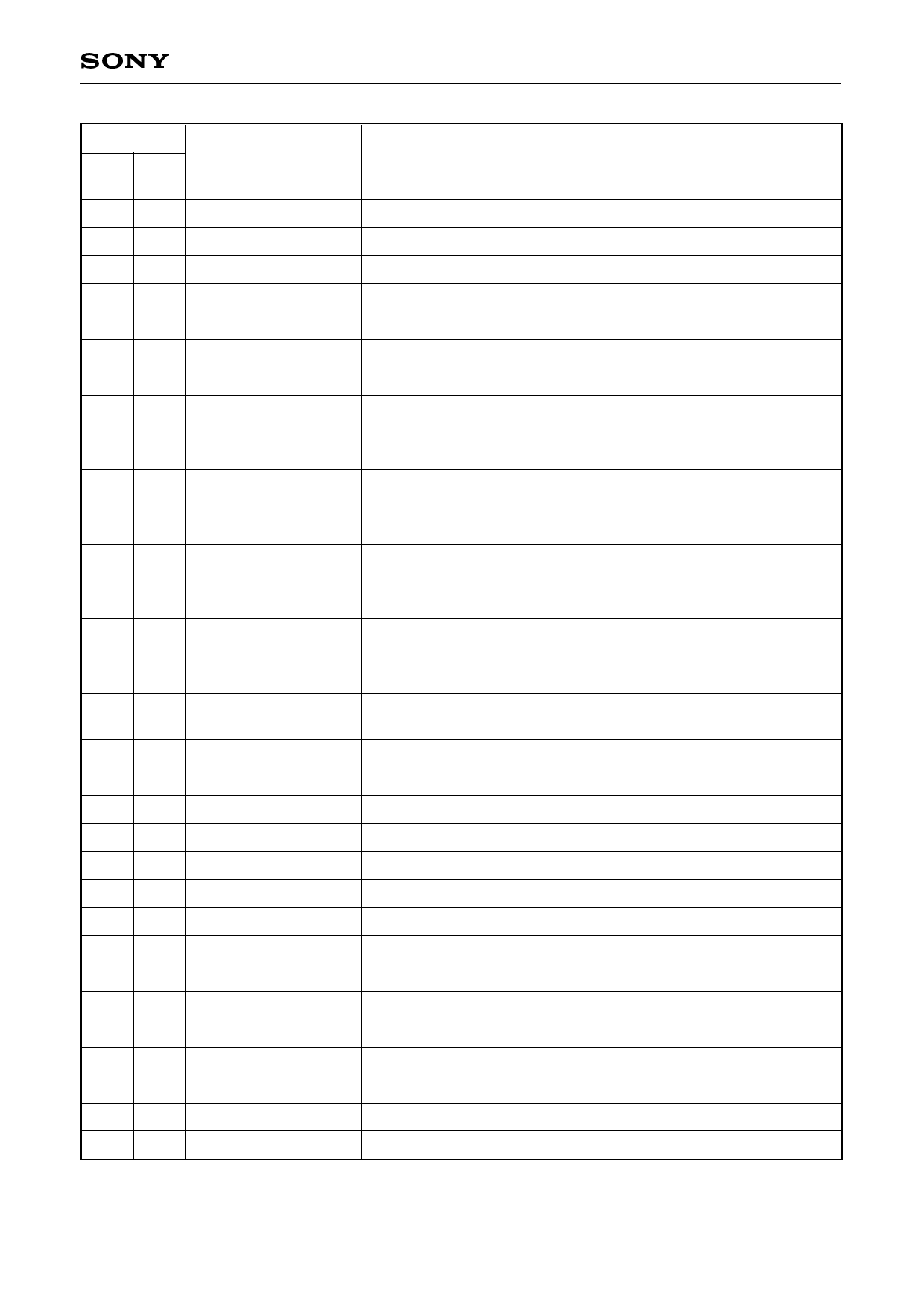
CXD2588Q/R
Pin No.
CXD CXD
2588R 2588Q
Symbol
70 72 V16M
71 73 VPCO
72 74 VSS
73 75 TES2
74 76 VDD
75 77 DOUT
76 78 LRCK
77 79 KRCKI
78 80 PCMD
79 81 PCMDI
80 82 BCK
81 83 BCKI
82 84 EMPH
83 85 EMPHI
84 86 XVDD
85 87 XTAI
86 88 XTAO
87 89 XVSS
88 90 AVDD1
89 91 AOUT1
90 92 AIN1
91 93 LOUT1
92 94 AVSS1
93 95 AVSS2
94 96 LOUT2
95 97 AIN2
96 98 AOUT2
97 99 AVDD2
98 100 RMUT
99 1 LMUT
100 2 NC
I/O
Output
values
Description
O 1, 0 Wide-band EFM PLL VCO2 oscillation output.
O 1, Z, 0 Wide-band EFM PLL charge pump output.
— — Digital GND.
I
Test pin. Normally GND.
— — Digital power supply.
O 1, 0 Digital Out output.
O 1, 0 D/A interface. LR clock output f = Fs.
I
D/A interface. LR clock input.
O
1, 0
D/A interface. Serial data output.
(two's complement, MSB first)
I
D/A interface. Serial data input.
(two's complement, MSB first)
O 1, 0 D/A interface. Bit clock output.
I
D/A interface. Bit clock input.
O
1, 0
Outputs a high signal when the playback disc has emphasis, and a
low signal when there is no emphasis.
I
Inputs a high signal when de-emphasis is on, and a low signal when
de-emphasis is off.
— — Master clock power supply.
I
Crystal oscillation circuit input. Master clock is externally input from
this pin.
O
Crystal oscillation circuit output.
— — Master clock GND.
— — Analog power supply.
O
L ch analog output.
I
L ch operational amplifier input.
O
L ch LINE output.
— — Analog GND.
— — Analog GND.
O
R ch LINE output.
I
R ch operational amplifier output.
O
R ch analog output.
— — Analog power supply.
O 1, 0 R ch zero detection flag.
O 1, 0 L ch zero detection flag.
–7–
Share Link: 