CXD2588R Ver la hoja de datos (PDF) - Sony Semiconductor
Número de pieza
componentes Descripción
Fabricante
CXD2588R Datasheet PDF : 121 Pages
| |||
CXD2588Q/R
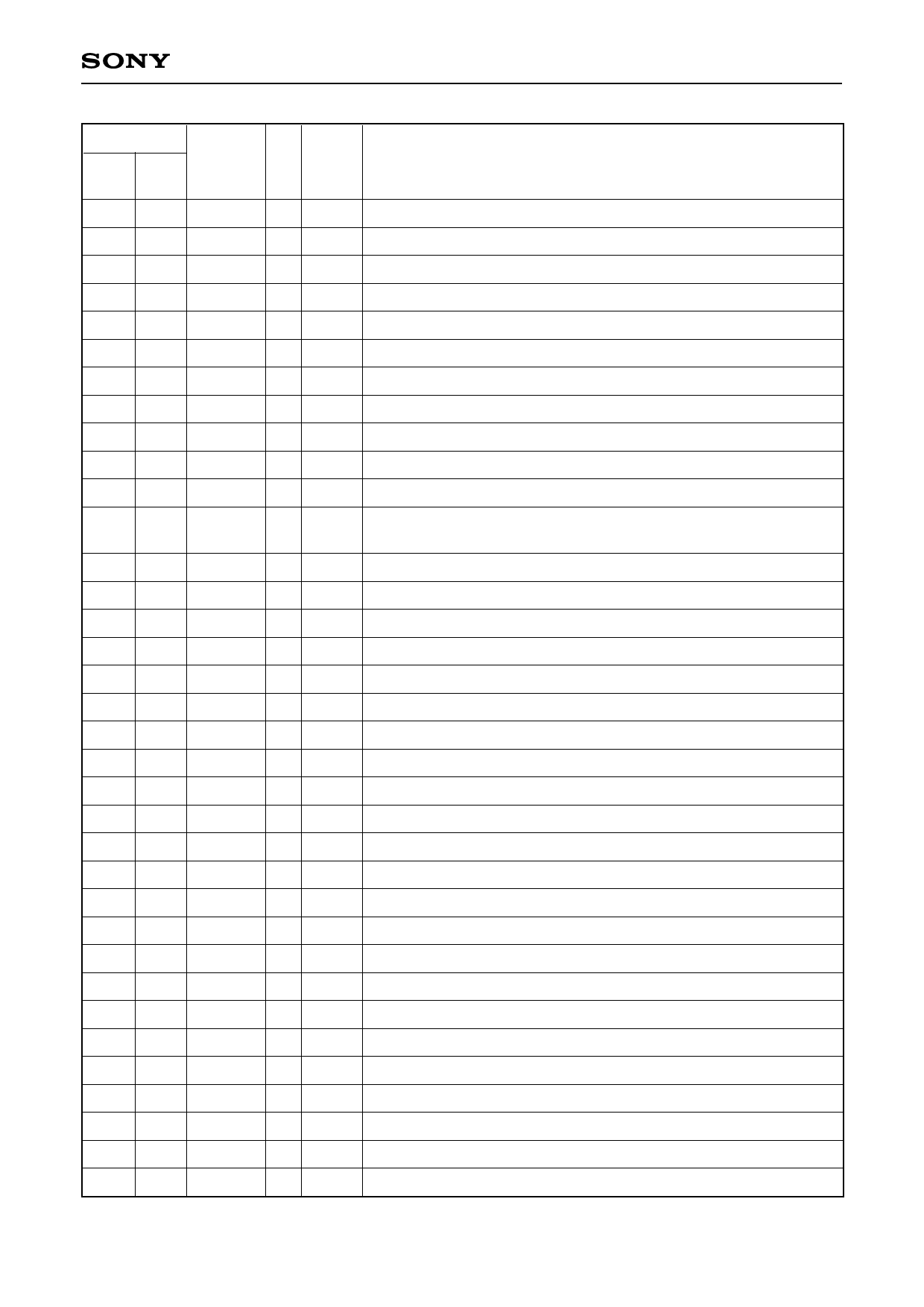
Pin No.
CXD CXD
2588R 2588Q
Symbol
35 37 FSTI
36 38 SFDR
37 39 SRDR
38 40 TFDR
39 41 TRDR
40 42 FFDR
41 43 FRDR
42 44 VSS
43 45 VSS
44 46 TEST
45 47 TES1
46 48 XTSL
47 49 VC
48 50 FE
49 51 SE
50 52 NC
51 53 TE
52 54 CE
53 55 RFDC
54 56 ADIO
55 57 AVSS0
56 58 IGEN
57 59 AVDD0
58 60 ASYO
59 61 ASYI
60 62 BIAS
61 63 RFAC
62 64 AVSS3
63 65 CLTV
64 66 FILO
65 67 FILI
66 68 PCO
67 69 AVDD3
68 70 VCTL
69 71 VCKI
I/O
Output
values
Description
I
2/3 frequency division input for XTAI pin.
O 1, 0 Sled drive output.
O 1, 0 Sled drive output.
O 1, 0 Tracking drive output.
O 1, 0 Tracking drive output.
O 1, 0 Focus drive output.
O 1, 0 Focus drive output.
— — Digital GND.
— — Digital GND.
I
Test pin. Normally, GND.
I
Test pin. Normally, GND.
I
Crystal selection input. Low when the crystal is 16.9344MHz; high
when the crystal is 33.8688MHz.
I
Center voltage input.
I
Focus error signal input.
I
Sled error signal input.
I
Tracking error signal input.
I
Center servo analog input.
I
RF signal input.
O Analog Test pin. No connected.
— — Analog GND.
I
Operational amplifier constant current input.
— — Analog power supply.
O 1, 0 EFM full-swing output. (low = Vss, high = VDD)
I
Asymmetry comparator voltage input.
I
Asymmetry circuit constant current input.
I
EFM signal input.
— — Analog GND.
I
Multiplier VCO1 control voltage input.
O Analog Master PLL filter output. (slave = digital PLL)
I
Master PLL filter input.
O 1, Z, 0 Master PLL charge pump output.
— — Analog power supply.
I
Wide-band EFM PLL VCO2 control voltage input.
I
Wide-band EFM PLL VCO2 oscillation input.
–6–
Share Link: 