CXD2588R Ver la hoja de datos (PDF) - Sony Semiconductor
Número de pieza
componentes Descripción
Fabricante
CXD2588R Datasheet PDF : 121 Pages
| |||
CXD2588Q/R
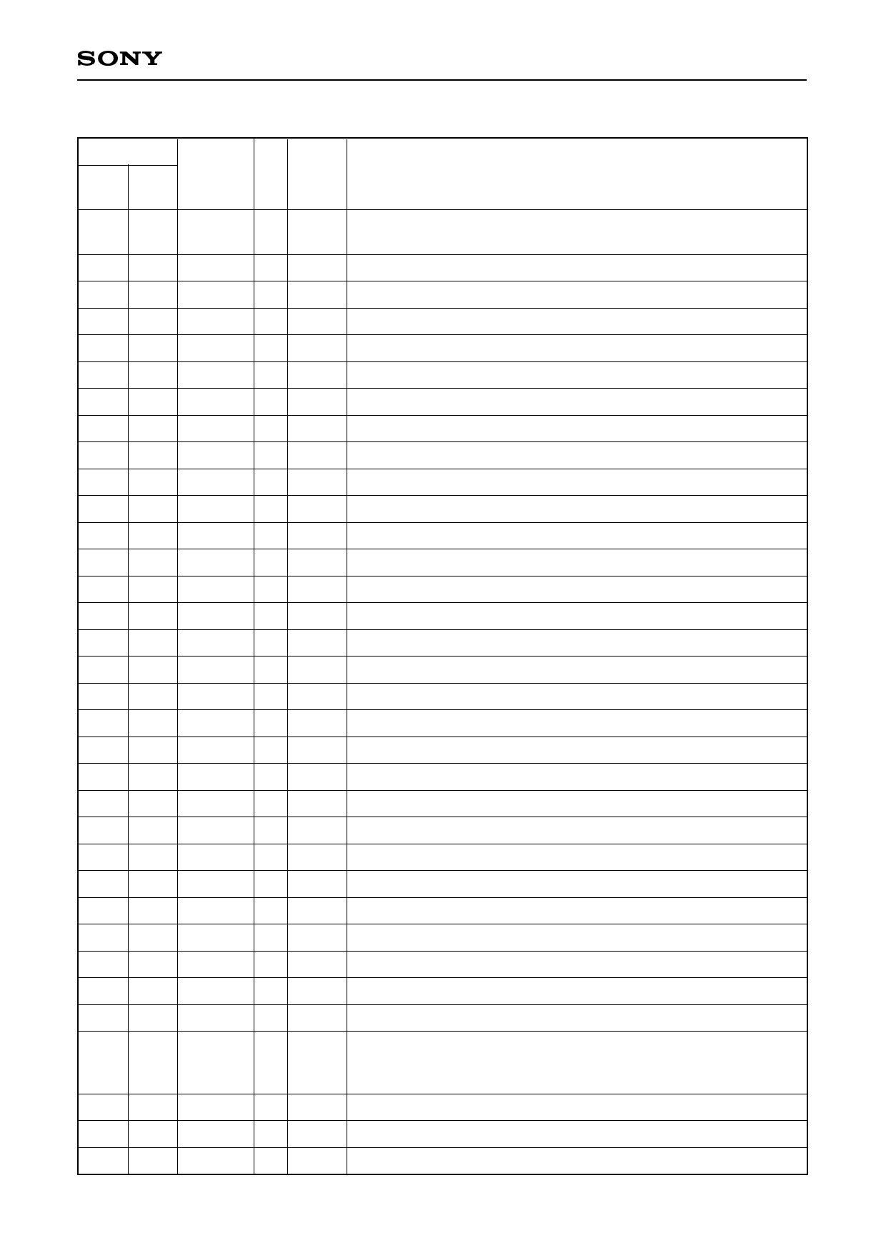
Pin Description
Pin No.
CXD CXD
2588R 2588Q
Symbol
1
3 SQSO
2
4 SQCK
3
5 SBSO
4
6 EXCK
5
7 XRST
6
8 SYSM
7
9 DATA
8 10 XLAT
9 11 CLOK
10 12 SENS
11 13 SCLK
12 14 PWMI
13 15 VDD
14 16 VDD
15 17 ATSK
16 18 SPOA
17 19 SPOB
18 20 XLON
19 21 WFCK
20 22 XUGF
21 23 XPCK
22 24 GFS
23 25 C2PO
24 26 SCOR
25 27 C4M
26 28 WDCK
27 29 COUT
28 30 MIRR
29 31 DFCT
30 32 FOK
31 33 LOCK
32 34 MDP
33 35 SSTP
34 36 FSTO
I/O
Output
values
Description
O
1, 0
Sub Q 80-bit, PCM peak and level data outputs. CD TEXT data
output.
I
SQSO readout clock input.
O 1, 0 Sub Q P to W serial output.
I
SBSO readout clock input.
I
System reset. Reset when low.
I
Mute input. Muted when high.
I
Serial data input from CPU.
I
Latch input from CPU. Serial data is latched at the falling edge.
I
Serial data transfer clock input from CPU.
O 1, 0 SENS output to CPU.
I
SENS serial data readout clock input.
I
Spindle motor external control input.
— — Digital power supply.
— — Digital power supply.
I/O 1, 0 Anti-shock input/output.
I
Microcomputer extension interface (input A)
I
Microcomputer extension interface (input B)
O 1, 0 Microcomputer extension interface (output)
O 1, 0 WFCK output.
O 1, 0 XUGF output. MINT1 or RFCK is output by switching with the command.
O 1, 0 XPCK output. MNT0 is output by switching with the command.
O 1, 0 GFS output. MNT3 or XROF is output by switching with the command.
O 1, 0 C2PO output. GTOP is output by switching with the command.
O 1, 0 Outputs a high signal when either subcode sync S0 or S1 is detected.
O 1, 0 4.2336MHz output. In CAV-W mode, 1/4 frequency division output for VCKI.
O 1, 0 Word clock output. f = 2Fs.
I/O 1, 0 Track count signal input/output.
I/O 1, 0 Mirror signal input/output.
I/O 1, 0 Defect signal input/output.
I/O 1, 0 Focus OK signal input/output.
GFS is sampled at 460Hz; when GFS is high, this pin outputs a
I/O 1, 0 high signal. If GFS is low eight consecutive samples, this pin
outputs low. Or input when LKIN = 1.
O 1, Z, 0 Spindle motor servo control output.
I
Disc innermost track detection signal input.
O 1, 0 2/3 frequency division output for XTAI pin.
–5–
Share Link: 