ICM7226A Ver la hoja de datos (PDF) - Harris Semiconductor
Número de pieza
componentes Descripción
Fabricante
ICM7226A Datasheet PDF : 18 Pages
| |||
ICM7226A, ICM7226B
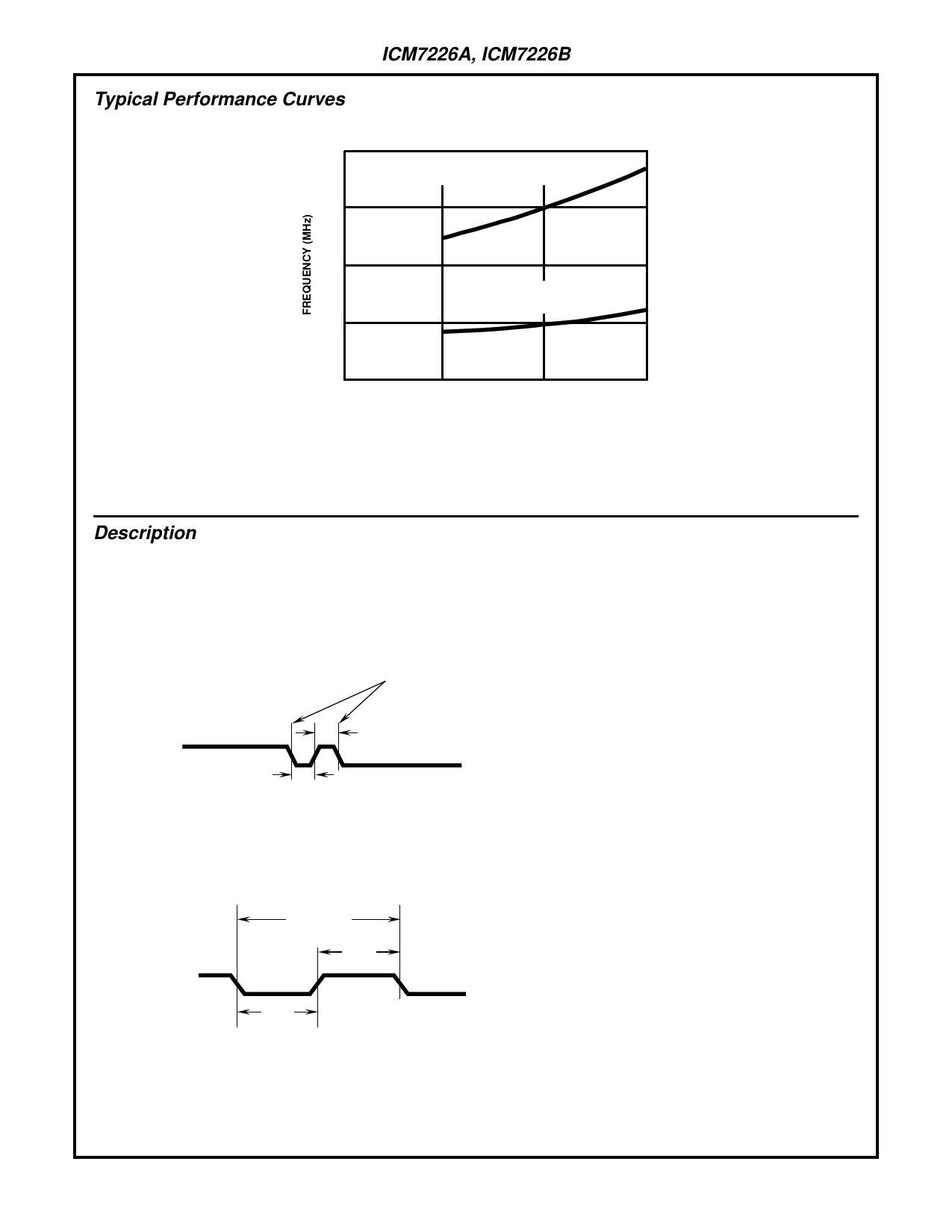
Typical Performance Curves (Continued)
20
fA (MAX) FREQUENCY UNIT COUNTER,
FREQUENCY RATIO MODES
15
10
fA (MAX) fB (MAX) PERIOD
TIME INTERVAL MODES
5
TA = +25oC
0
3
4
5
6
VDD-VSS (V)
FIGURE 8. fA(MAX), fB(MAX) AS A FUNCTION OF SUPPLY
Description
INPUTS A and B
The signal to be measured is applied to INPUT A in fre-
quency period, unit counter, frequency ratio and time interval
modes. The other input signal to be measured is applied to
INPUT B in frequency ratio and time interval. fA should be
higher than fB during frequency ratio.
COUNTED
TRANSITIONS
Both inputs are digital inputs with a typical switching thresh-
old of 2.0V at VDD = 5.0V and input impedance of 250kΩ.
For optimum performance, the peak to peak input signal
should be at least 50% of the supply voltage and centered
about the switching voltage. When these inputs are being
driven from TTL logic, it is desirable to use a pullup resistor.
The circuit counts high to low transitions at both inputs
INPUT A 4.5V
0.5V
50ns MIN
50ns MIN
tR = tF = 10ns
Note that the amplitude of the input should not exceed the
device supply (above the VDD and below the VSS) by more
than 0.3V, otherwise the device may be damaged.
Multiplexed Inputs
FIGURE 9. WAVEFORM FOR GUARANTEED MINIMUM fA(MAX)
FUNCTION = FREQUENCY, FREQUENCY RATIO,
UNIT COUNTER
INPUT A OR 4.5V
INPUT B 0.5V
MEASURED
INTERVAL
250ns
MIN
250ns
MIN
tR = tF = 10s
FIGURE 10. WAVEFORM FOR GUARANTEED MINIMUM fB(MAX)
AND fA(MAX) FOR FUNCTION = PERIOD AND TIME
INTERVAL
The FUNCTION, RANGE, CONTROL and EXTERNAL
DECIMAL POINT inputs are time multiplexed to select the
function desired. This is achieved by connecting the appro-
priate Digit driver output to the inputs. The function, range
and control inputs must be stable during the last half of each
digit output, (typically 125µs). The multiplexed inputs are
active high for the common anode lCM7226A and active low
for the common cathode lCM7226B.
Noise on the multiplex inputs can cause improper operation.
This is particularly true when the unit counter mode of oper-
ation is selected, since changes in voltage on the digit driv-
ers can be capacitively coupled through the LED diodes to
the multiplex inputs. For maximum noise immunity, a 10kΩ
resistor should be placed in series with the multiplexed
inputs as shown in the application circuits.
13-70
Share Link: 